PCB Design Guidelines (HSSI, EMIF, MIPI, True Differential, PDN) User Guide: Agilex™ 5 FPGAs and SoCs
ID
821801
Date
12/08/2025
Public
1. Overview
2. BGA Footprint and Land Pattern
3. General PCB Design Considerations
4. VPBGA PCB Routing Guidelines
5. MBGA PCB Routing Guidelines
6. EMIF PCB Routing Guidelines (VPBGA and MBGA)
7. MIPI Interface Layout Design Guidelines (VPBGA and MBGA)
8. True Differential I/O Interface PCB Routing Guidelines (VPBGA and MBGA)
9. Power Distribution Network Design Guidelines
10. Document Revision History for the PCB Design Guidelines (HSSI, EMIF, MIPI, True Differential, PDN) User Guide: Agilex™ 5 FPGAs and SoCs
9.1. Agilex™ 5 Power Distribution Network Design Guidelines Overview
9.2. Power Delivery Overview
9.3. Board Power Delivery Network Recommendations
9.4. Board LC Recommended Filters for Noise Reduction in Combined Power Delivery Rails
9.5. PCB PDN Design Guideline for Unused GTS Transceiver
9.6. PCB Voltage Regulator Recommendation for PCB Power Rails
9.7. Board PDN Simulations
9.8. Agilex™ 5 Device Family PDN Design Summary
9.3.1. Board Decoupling Capacitors Guide
In addition to on-package decoupling (OPD) (as land-side capacitor (LSC) and die-side capacitor (DSC)), the Agilex™ 5 device family also offers a bottom side and periphery capacitors (refer to the Agilex™ 5 FPGA Packages Board-Level Decoupling Capacitors Summary section, the bottom side capacitors for each power rail) can be added into the Agilex™ 5 E-Series Group B modular development kit (SoM) as shown in the following figures.
Figure 75. Bottom Side Decoupling Capacitors and the Use of PTH ViaThis figure shows an example of decoupling capacitors placed on the bottom side for a PCB designed for the Agilex™ 5 E-Series Group B modular development kit (SoM) without socket and the use of PTH via.
Figure 76. Periphery Decoupling Capacitors and the Use of PTH ViaThis figure shows an example of periphery decoupling capacitors for a PCB designed for the Agilex™ 5 E-Series Group B modular development kit (SoM) without socket and the use of PTH via.
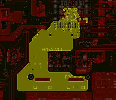
Considering the VPBGA mapping, Altera recommends that you include a power flood on the bottom layer of the board for VCCL.
Figure 77. Example of Board Power Flooding This figure shows a good design practice to reduce the loop inductance caused by a shorter path to the FPGA fabric and more effective decoupling solution.