Multi Channel DMA Intel® FPGA IP for PCI Express User Guide
A newer version of this document is available. Customers should click here to go to the newest version.
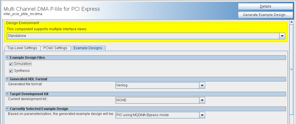
6.4. Example Designs
| Parameter | Value | Default Value | Description |
|---|---|---|---|
| Simulation |
On / Off |
True |
When Simulation box is checked, all necessary filesets required for simulation are generated. When this box is NOT checked, filesets required for Simulation are NOT generated. Instead a Platform Designer example design system is generated.
Note: Multiple physical functions and SR-IOV are not supported for simulation. When you generate an example design, turn off Simulation.
|
| Synthesis |
On / Off |
True |
When Synthesis box is checked, all necessary filesets required for synthesis are generated. When Synthesis box is NOT checked, filesets required for Synthesis are NOT generated. Instead a Platform Designer example design system is generated |
| Generated file format |
Verilog |
Verilog |
HDL format |
| Current development kit |
None MCDMA P-Tile IP:
MCDMA F-Tile IP:
|
This option provides supports for various Development Kits listed. The details of Intel FPGA Development kits can be found on Intel FPGA website. If this menu is grayed out, it is because no board is supported for the options selected (for example, synthesis deselected). If an Intel FPGA Development board is selected, the Target Device used for generation is the one that matches the device on the Development Kit |
|
| Currently Selected Example Design |
PIO using MQDMA Bypass mode Device-side Packet Loopback Packet Generate/Check AVMM DMA Traffic Generator/Checker External Descriptor Controller |
Based on MCDMA setting for "User Mode" and "Interface Type" different Example Designs are supported. List of Example design options are: User Mode=MCDMA, Interface Type=AVST:
User Mode=MCDMA, Interface Type=AVMM:
User Mode=Bursting Master:
User Mode=BAM+BAS:
User Mode=BAM+MCDMA, Interface Type=AVMM:
User Mode=BAM+MCDMA, Interface Type=AVST:
User Mode=Data Mover Only:
|