Cyclone® V Avalon® Memory-Mapped (Avalon-MM) Interface for PCI Express* Solutions User Guide
ID
683494
Date
10/24/2024
Public
1. Datasheet
2. Getting Started with the Avalon-MM Cyclone V Hard IP for PCI Express
3. Parameter Settings
4. Interfaces and Signal Descriptions
5. Registers
6. Reset and Clocks
7. Interrupts for Endpoints
8. Error Handling
A. PCI Express Protocol Stack
9. Design Implementation
10. Additional Features
11. Transceiver PHY IP Reconfiguration
12. Debugging
B. Frequently Asked Questions for PCI Express
C. Lane Initialization and Reversal
D. Document Revision History
2.1. Running Platform Designer
2.2. Generating the Example Design
2.3. Running a Gate-Level Simulation
2.4. Simulating the Single DWord Design
2.5. Understanding Channel Placement Guidelines
2.6. Generating Synthesis Files
2.7. Compiling the Design in the Quartus® Prime Software
2.8. Programming a Device
5.1. Correspondence between Configuration Space Registers and the PCIe Specification
5.2. Type 0 Configuration Space Registers
5.3. Type 1 Configuration Space Registers
5.4. PCI Express Capability Structures
5.5. Intel-Defined VSEC Registers
5.6. CvP Registers
5.7. 64- or 128-Bit Avalon-MM Bridge Register Descriptions
5.8. Programming Model for Avalon-MM Root Port
5.9. Uncorrectable Internal Error Mask Register
5.10. Uncorrectable Internal Error Status Register
5.11. Correctable Internal Error Mask Register
5.12. Correctable Internal Error Status Register
5.7.1.1. Avalon-MM to PCI Express Interrupt Status Registers
5.7.1.2. Avalon-MM to PCI Express Interrupt Enable Registers
5.7.1.3. PCI Express Mailbox Registers
5.7.1.4. Avalon-MM-to-PCI Express Address Translation Table
5.7.1.5. PCI Express to Avalon-MM Interrupt Status and Enable Registers for Endpoints
5.7.1.6. Avalon-MM Mailbox Registers
5.7.1.7. Control Register Access (CRA) Avalon-MM Slave Port
A.4.1. Avalon‑MM Bridge TLPs
A.4.2. Avalon-MM-to-PCI Express Write Requests
A.4.3. Avalon-MM-to-PCI Express Upstream Read Requests
A.4.4. PCI Express-to-Avalon-MM Read Completions
A.4.5. PCI Express-to-Avalon-MM Downstream Write Requests
A.4.6. PCI Express-to-Avalon-MM Downstream Read Requests
A.4.7. Avalon-MM-to-PCI Express Read Completions
A.4.8. PCI Express-to-Avalon-MM Address Translation for 32-Bit Bridge
A.4.9. Minimizing BAR Sizes and the PCIe Address Space
A.4.10. Avalon® -MM-to-PCI Express Address Translation Algorithm for 32-Bit Addressing
2.1. Running Platform Designer
- Launch the Quartus® Prime software. Alternatively, you can also use the Quartus Prime Lite Edition software.
- On the File menu, select New, then Platform Designer System File.
- Open the ep_g1x4.qsys example design.
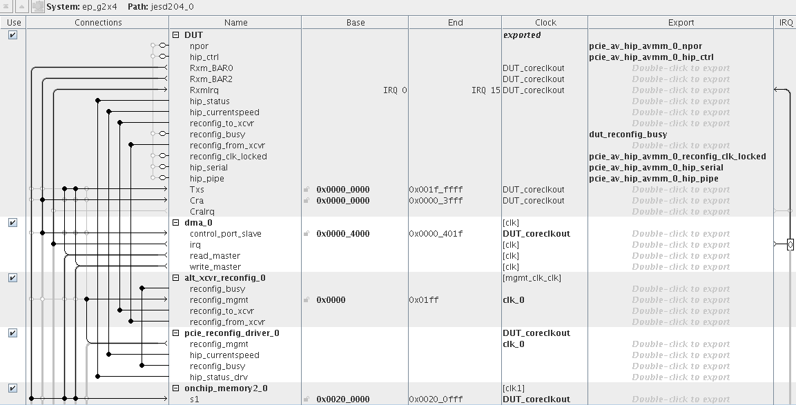
The following figure shows a Platform Designer system that includes the Transceiver Reconfiguration Controller and the Altera PCIe Reconfig Driver IP Cores. The Transceiver Reconfiguration Controller performs dynamic reconfiguration of the analog transceiver settings to optimize signal quality. You must include these components to the Platform Designer system to run successfully in hardware.
Figure 5. Platform Designer Avalon-MM Design for PCIe with Transceiver Reconfiguration Components
Refer to Creating a System with Platform Designer in volume 1 of the Quartus® Prime Handbook for more information about how to use Platform Designer. For an explanation of each Platform Designer menu item, refer to About Platform Designer in the Quartus® Prime Help.