AN 766: Intel® Stratix® 10 Devices, High Speed Signal Interface Layout Design Guideline
ID
683132
Date
3/12/2019
Public
Intel® Stratix® 10 Devices and Transceiver Channels
PCB Stackup Selection Guideline
Recommendations for High Speed Signal PCB Routing
FPGA Fan-out Region Design
CFP2/CFP4 Connector Board Layout Design Guideline
QSFP+/zSFP/QSFP28 Connector Board Layout Design Guideline
SMA 2.4-mm Layout Design Guideline
Tyco/Amphenol Interlaken Connector Design Guideline
Electrical Specifications
Document Revision History for AN 766: Intel® Stratix® 10 Devices, High Speed Signal Interface Layout Design Guideline
Option 1: Via-In-Pad Topology
Option 2: Dog-bone with GND Cutout at BGA Pad Topology
Option 3: Micro-via Topology
GND Cutout Under BGA Pads in Fan-out Configuration
Comparison of Dog-bone with GND Cutout Under the BGA and Via-in-Pad Configurations
Trace Shape Routing at the BGA Void Area (Tear Drop Configuration)
Signal Break-out Recommendations
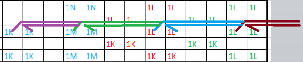
Figure Figure 3 shows that there are up to 4 transceiver pairs in one row for Intel® Stratix® 10 devices. Designers must assign at least 4 signals layers each separated by continuous ground planes for break-out routing. The number of layers assigned for transceivers routing is one of the key factors for stackup selection. Intel recommends that you follow FPGA break-out region guideline in the next section to achieve optimum performance.
Figure 3. Example of Recommended FPGA Break-Out Routing (Different colors stands for different layers)
There are three options for FPGA fan-out region routing. Each one can be selected for high speed signal routing on PCB, based on their high priority and data rate.
Note: Intel recommends BGA pad diameter on PCB as 20 mil for Intel® Stratix® 10 devices. This is good for pads that are not near the corners of the device. However, for those five pads which are located closest to each corner of device, the recommended pad diameter is 24 mil with 20 mil solder mask opening for inner pins and 16 mil for corner pins.
- Option 1: Via-In-Pad Topology
- Option 2: Dog-bone with GND Cutout at BGA Pad Topology
- Option 3: Micro-via Topology
- GND Cutout Under BGA Pads in Fan-out Configuration
- Comparison of Dog-bone with GND Cutout Under the BGA and Via-in-Pad Configurations
- Trace Shape Routing at the BGA Void Area (Tear Drop Configuration)