AN 766: Intel® Stratix® 10 Devices, High Speed Signal Interface Layout Design Guideline
QSFP28 Example Design and Performance Optimization
This section describes the optimization performed at the connector for the best insertion and return loss and crosstalk (isolation) performances of the channel.
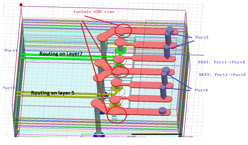
In the figure above, the signal finished drill size is 8 mil, the via pad is 18 mil, and the rectangular differential via-anti-pad is 45 mil x 80 mil. The signal via to signal via pitch in one pair is 40 mil. The signal via to GND via pitch is 27 mil. Routing is on layer 5. All signal vias are back-drilled up to layer 6.
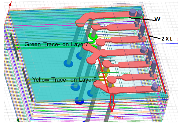
The reference design is considered without the GND cutout below the connector pads (blue reference design in Figure 80). The performance in Figure 79 is observed by using various GND cutout (W) mil x (L) mil below each transceiver pair. W is swept from 50 mil to 100 mil and L from 65 mil to 110 mil. The GND cutout had been applied only on GND layer#2 as shown in Figure 79
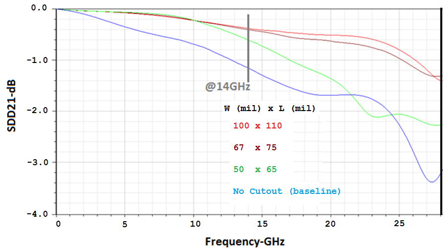
In the figure above, the differential return loss performance is from the stripline trace ports.
The green design features a GND cutout at 50 mil x 65 mil.
The brown design features a GND cutout at 67 mil x 75 mil.
Intel recommends the red design which features a GND cutout at 100 mil x 110 mil.
The green design features a GND cutout at 50 mil x 65 mil.
The brown design features a GND cutout at 67 mil x 75 mil.
The red design features a GND cutout at 100 mil x 110 mil.
Intel recommends the red design which features a GND cutout at 100 mil x 110 mil.
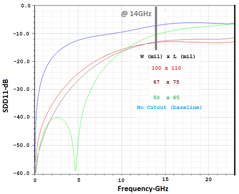
The figures above indicate that the recommended GND cutout has the best performance compared to all the others.
To further optimize the layout structure in Figure 79, two GND reference diving boards for stripline trace routing have been added.
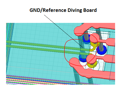
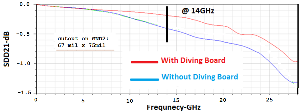
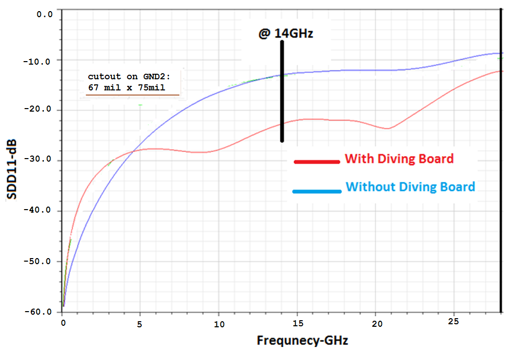
The addition of reference diving boards enhances both insertion and return loss performance.
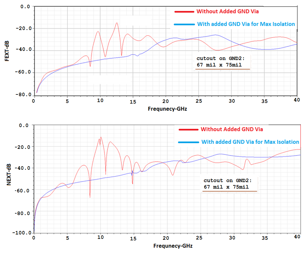
To improve isolation between the two pairs, you can insert an additional GND via between the signal pairs. Most of the crosstalk will occur through vertical coupling between signal vias of two different signal pairs. Therefore, adding one GND via will enhance the isolation.