AN 766: Intel® Stratix® 10 Devices, High Speed Signal Interface Layout Design Guideline
ID
683132
Date
3/12/2019
Public
Intel® Stratix® 10 Devices and Transceiver Channels
PCB Stackup Selection Guideline
Recommendations for High Speed Signal PCB Routing
FPGA Fan-out Region Design
CFP2/CFP4 Connector Board Layout Design Guideline
QSFP+/zSFP/QSFP28 Connector Board Layout Design Guideline
SMA 2.4-mm Layout Design Guideline
Tyco/Amphenol Interlaken Connector Design Guideline
Electrical Specifications
Document Revision History for AN 766: Intel® Stratix® 10 Devices, High Speed Signal Interface Layout Design Guideline
Option 1: Via-In-Pad Topology
Option 2: Dog-bone with GND Cutout at BGA Pad Topology
Option 3: Micro-via Topology
GND Cutout Under BGA Pads in Fan-out Configuration
Comparison of Dog-bone with GND Cutout Under the BGA and Via-in-Pad Configurations
Trace Shape Routing at the BGA Void Area (Tear Drop Configuration)
Recommended PCB layout Design for Version-B SMA 2.4 mm Connector
An optimized layout suppresses the natural cavity mode within the via GND ring as well as additional cavity coupling to other structures on the PCB.
Figure 90. Version-B 2.4 mm Connector LaunchThe diameter of the signal via drill hole is 10 mil.

D1: diameter of the signal anti-pad on the top layer = 60 mil.
D2: diameter of the signal pad = 20 mil.
D3: diameter of the signal anti-pad on the inner layers = 40 mil.
D4: diameter selected = 118 mil.
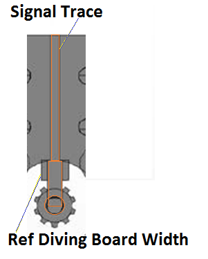
The width of the reference diving board must be at least twice the width of the signal trace.
Figure 91. Magnified Signal Trace and Reference Plane Areas at the Connector