AN 766: Intel® Stratix® 10 Devices, High Speed Signal Interface Layout Design Guideline
ID
683132
Date
3/12/2019
Public
Intel® Stratix® 10 Devices and Transceiver Channels
PCB Stackup Selection Guideline
Recommendations for High Speed Signal PCB Routing
FPGA Fan-out Region Design
CFP2/CFP4 Connector Board Layout Design Guideline
QSFP+/zSFP/QSFP28 Connector Board Layout Design Guideline
SMA 2.4-mm Layout Design Guideline
Tyco/Amphenol Interlaken Connector Design Guideline
Electrical Specifications
Document Revision History for AN 766: Intel® Stratix® 10 Devices, High Speed Signal Interface Layout Design Guideline
Option 1: Via-In-Pad Topology
Option 2: Dog-bone with GND Cutout at BGA Pad Topology
Option 3: Micro-via Topology
GND Cutout Under BGA Pads in Fan-out Configuration
Comparison of Dog-bone with GND Cutout Under the BGA and Via-in-Pad Configurations
Trace Shape Routing at the BGA Void Area (Tear Drop Configuration)
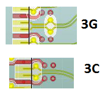
Two Different Break-out Routings at the CFP4 Connector Area
Figure 57. Two Different Break-out Routings at the CFP4 Connector AreaThe 3C configuration is what has been previously recommended. The 3G configuration is a different way of routing while the signal vias are moved away from the connector pads to allow more space for break-out routing.
The main PCB routing differential impedance is designed for 95 Ω as was previously recommended.
Figure 58. TDR Performance from the CFP4 Connector Pad on the PCB
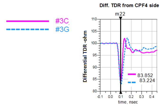
The measured TDR from the connector pads show no appreciable difference.
The total length of 3C is 60 mil larger than 3G.
Note: Intel recommends that you not have two GND vias assigned for one signal via as seen in 3C above.