AN 766: Intel® Stratix® 10 Devices, High Speed Signal Interface Layout Design Guideline
Performance Comparison between Option1 and Option2 layout
A version-B SMA connector model in figure Version-B Molex 2.4 mm SMA connector has been implemented on both layout design recommendations Option1 and Option2 in figure Recommended layout for Molex Version-A 2.4 mm SMA connector and figure Version-B 2.4 mm Connector Launch respectively. Only the Connector model and a small portion of Host PCB has been included into this simulation and performance comparison. Both simulations are using similar stack up materials and the main PCB routing is on layer 7. There is slight difference of about 6 mil in signal via height (Signal via height in Option 1 layout is about 6 mil more than that in Option 2). From Insertion loss point of via, there is about 0.18 dB difference at 14 GHz as shown in figure Single ended Insertion loss comparison for Version-B SMA connector on both recommended Option1 and Option2 layout design. (Improved by 0.18 dB at 14 GHz) .
Option 1 = Recommended PCB layout Design for Version-A SMA 2.4 mm Connector.
Option 2 = Recommended PCB layout Design for Version-B SMA 2.4 mm Connector.
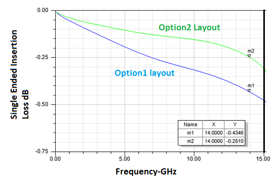
Insertion loss from the point of the via improves by approximately 0.18 dB at 14 GHz.
Option 1 = Recommended PCB layout Design for Version-A SMA 2.4 mm Connector.
Option 2 = Recommended PCB layout Design for Version-B SMA 2.4 mm Connector.
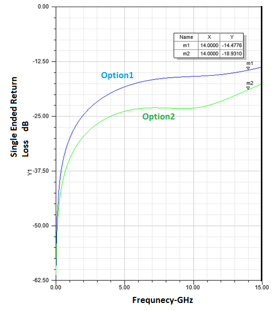
Return loss from the point of the connector port improves by 4.5 dB at 14 GHz.