AN 766: Intel® Stratix® 10 Devices, High Speed Signal Interface Layout Design Guideline
ID
683132
Date
3/12/2019
Public
Intel® Stratix® 10 Devices and Transceiver Channels
PCB Stackup Selection Guideline
Recommendations for High Speed Signal PCB Routing
FPGA Fan-out Region Design
CFP2/CFP4 Connector Board Layout Design Guideline
QSFP+/zSFP/QSFP28 Connector Board Layout Design Guideline
SMA 2.4-mm Layout Design Guideline
Tyco/Amphenol Interlaken Connector Design Guideline
Electrical Specifications
Document Revision History for AN 766: Intel® Stratix® 10 Devices, High Speed Signal Interface Layout Design Guideline
Option 1: Via-In-Pad Topology
Option 2: Dog-bone with GND Cutout at BGA Pad Topology
Option 3: Micro-via Topology
GND Cutout Under BGA Pads in Fan-out Configuration
Comparison of Dog-bone with GND Cutout Under the BGA and Via-in-Pad Configurations
Trace Shape Routing at the BGA Void Area (Tear Drop Configuration)
Recommended PCB Design Guideline for QSFP+/zQSFP/QSFP28 Channels
Figure 77. Recommended PCB Layout at the QSFP+ Connector Figure also applies to zQSFP and QSFP28 connectors on a PCB (host) operating up to 28 Gbps.
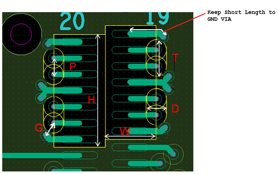
The yellow portions indicate GND2/GND4 cutout dimensions under the connector pads on the 1st and 2nd reference planes, respectively.
- Rectangular (W x H) cutout on the GN02 2 layer (recommended for data rates up to 17 Gbps) under the QSFP+ pads. For data rates up to 28 Gbps, add one additional GND layer cutout (GND04). W = 100 mil, H = 210 mil.
- Signal and GND vias, finished drill diameter = 10 mil, Via pad diameter = 20 mil
- All signal vias are back-drilled
- Each signal via must have one single GND via
- If the stack-up height is less than 1:12, you can also use an 8-mil finished via drill and an 18 mil via pad instead.
- P (signal-to-signal via pitch) = 40 mil
- Signal anti-pads: T = 90 mil, D = 45 mil
- G (signal-to-GND via pitch) = 30 mil
- 95 Ω differential PCB routing
Intel recommends that you have both the signal via and GND via located close enough to the connectors' signal and GND pads, respectively, to avoid cavity resonance at higher frequencies.
2 GN02/GND04 represents the first and second GND layers below the connector.