AN 766: Intel® Stratix® 10 Devices, High Speed Signal Interface Layout Design Guideline
CFP4 Connector Routing Topologies Design Example
In the figure below, notice that the CFP4 connector has not been included in simulations. The standard 24-layer stack-up at 117 mil thickness is used for this design example. The stack-up material is Megron6 and has eight signal layers and four PDR layers.
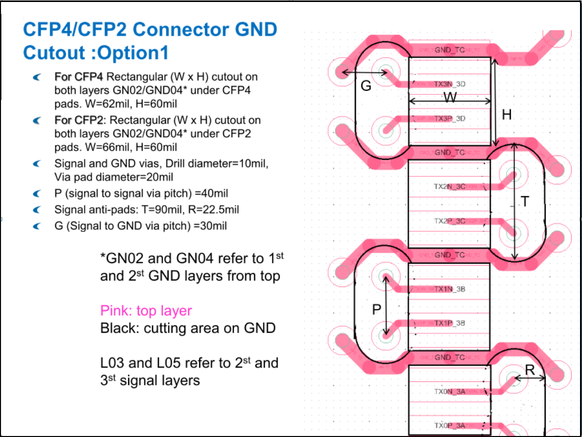

The channel trace routing is on layer 5 for both of the pairs above. Pair1 has two GND cutouts (on layers 2 and 4) under the connector pads, while pair1 has only one GND cutout on layer 2.
The reason for not having a GND cutout on layer 4 for pair 2 is because trace routing needs a reference GND plane while routed and passed under the connector pads. This aids in obtaining a minimum channel path as opposed to breaking out of the opposite direction and looping back, which creates a longer channel path.
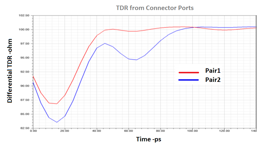
The following figures compare the performances of pair 1 and pair 2.

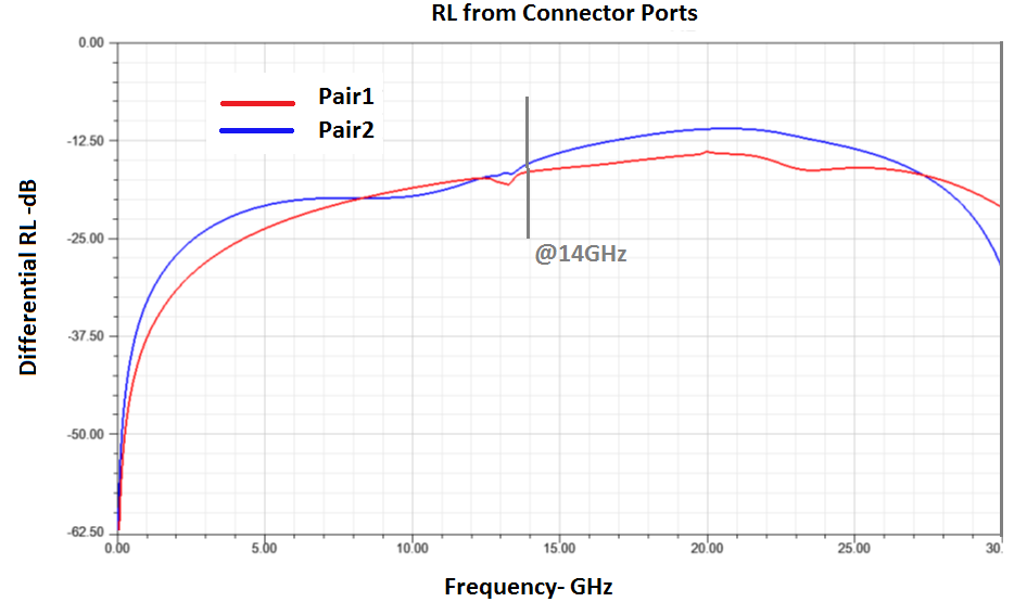
A quick comparison shows that pair 2 has up to 0.2 dB more insertion loss within a 15 GHz bandwidth. This is due to the lack of a GND cutout on layer 4 under the connector pads in addition to the extra routing length under the connector pads. Pair 2 also has up to 2.5 dB return loss with a 15 GHz bandwidth.
The TDR differential impedance also shows less impedance mismatch for pair 1.
In the following figure, the layout configuration has been changed from pair 2 (in the previous example) to pair 3.
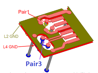
In the example above, pair 3 signal vias have been moved to the left side. This allows an additional GND cutout on layer 4 for pair 2 below the CFP4 connector pads. In this configuration, pair 3 can be routed on signal layer 3. The total routing length for both pair 1 and pair 3 are now equal.
The following figures compare the performances of pair 2 and pair 3.


The insertion and return loss results above show better performance for pair 2 within a 15 GHz bandwidth. This is due to a larger GND cutout below the CFP4 connector pads (combined rectangular cut out and signal via anti-pads). This is also observed from TDR differential impedance results. However, above 15 GHz, pair 2 in Figure 60 exhibits greater performance degradation than pair3 in Figure 64.