AN 766: Intel® Stratix® 10 Devices, High Speed Signal Interface Layout Design Guideline
ID
683132
Date
3/12/2019
Public
Intel® Stratix® 10 Devices and Transceiver Channels
PCB Stackup Selection Guideline
Recommendations for High Speed Signal PCB Routing
FPGA Fan-out Region Design
CFP2/CFP4 Connector Board Layout Design Guideline
QSFP+/zSFP/QSFP28 Connector Board Layout Design Guideline
SMA 2.4-mm Layout Design Guideline
Tyco/Amphenol Interlaken Connector Design Guideline
Electrical Specifications
Document Revision History for AN 766: Intel® Stratix® 10 Devices, High Speed Signal Interface Layout Design Guideline
Option 1: Via-In-Pad Topology
Option 2: Dog-bone with GND Cutout at BGA Pad Topology
Option 3: Micro-via Topology
GND Cutout Under BGA Pads in Fan-out Configuration
Comparison of Dog-bone with GND Cutout Under the BGA and Via-in-Pad Configurations
Trace Shape Routing at the BGA Void Area (Tear Drop Configuration)
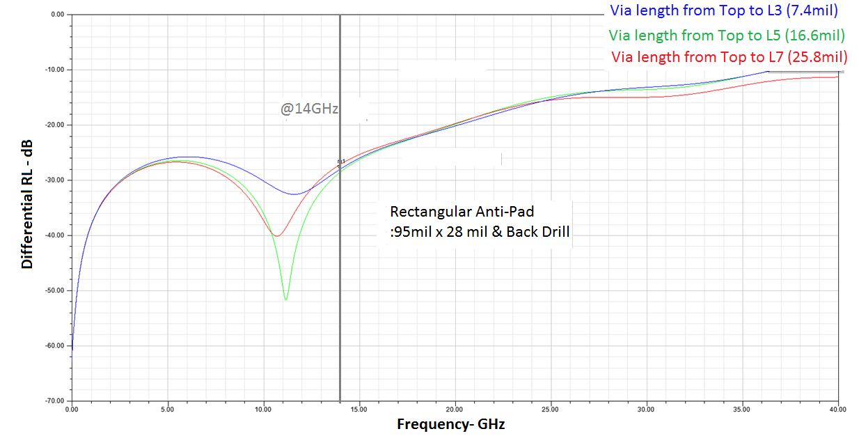
The Impact of Via Height and Via Anti-pad Over Insertion Loss
This section demonstrates how much via length and anti-pad size change the insertion loss. The results of this examination are based on the following criteria:
- A 24-layer stackup
- A via-in-pad with a 10 mil drill (finished size) hole
- 18 mil pad
Figure 34. 24-Layer Stack-up Information for investigations on insertion loss impact using various via lengths and anti-pad sizes.
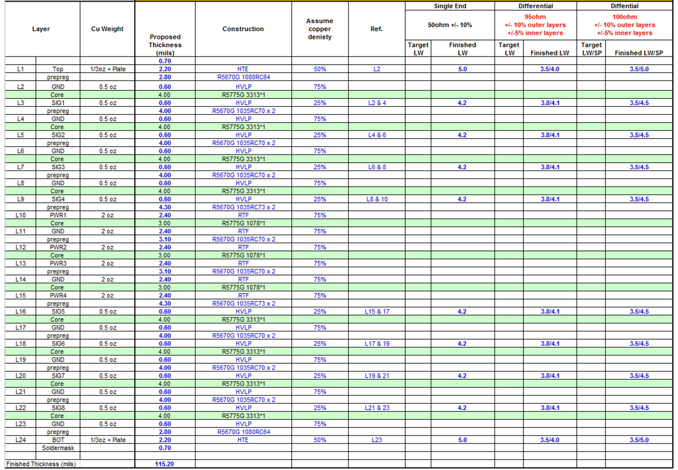
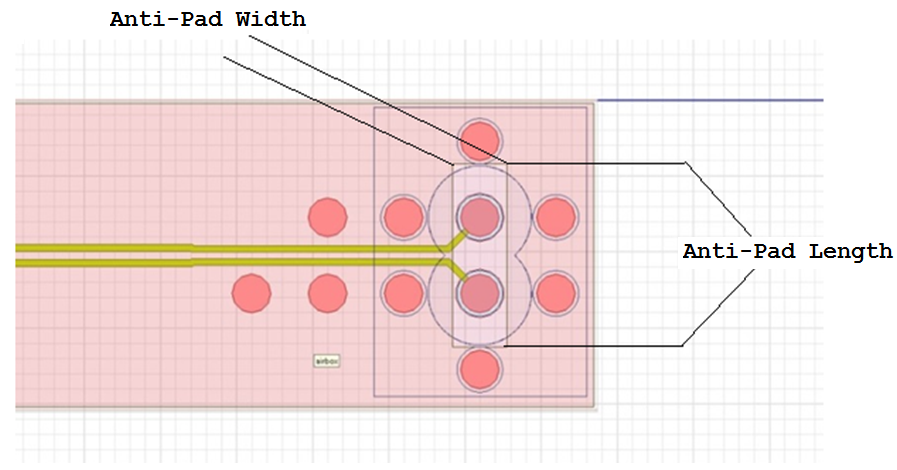
Figure 35. Differential Via and Anti-pad Configuration
| Case | Insertion Loss @ 14 GHz | Return Loss @14 GHz, ~ dB |
| Via length from top to L3 (7.4 mil) | -0.1730 dB | -29 |
| Via length from top to L5 (16.6 mil) | -0.1768 dB | -28 |
| Via length from top to L7 (25.8 mil) | -0.1828 dB | -27 |
Figure 36. Impact on Differential Insertion Loss by Via Length (SDD21)
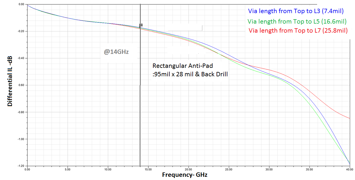
Figure 37. Impact on Differential Return Loss by Via Length (SDD11)
| Case | GND02 Cutout Size | GND04 Cutout Size | IL 14 GHz |
| 1A | 68 mil x 28 mil | 68 mil x 28 mil | -0.1988 dB |
| 2A | 95 mil x 28 mil | 95 mil x 28 mil | -0.1730 dB |
| Case/Cutout | GND02 | GND04 | GND06 | IL @14 GHz |
| 1B | 95 mil x 28 mil | 95 mil x 28 mil | 95 mil x 28 mil | -0.1768 dB |
| 2B | 95 mil x 50 mil | 95 mil x 50 mil | 95 mil x 50 mil | -0.1741 dB |
The signal anti-pad size results in these tables demonstrates that the larger the anti-pad, the less insertion and return loss results. Because space is always a consideration, you must balance the signal anti-pad size with the need for proper break-out routing.