AN 766: Intel® Stratix® 10 Devices, High Speed Signal Interface Layout Design Guideline
ID
683132
Date
3/12/2019
Public
Intel® Stratix® 10 Devices and Transceiver Channels
PCB Stackup Selection Guideline
Recommendations for High Speed Signal PCB Routing
FPGA Fan-out Region Design
CFP2/CFP4 Connector Board Layout Design Guideline
QSFP+/zSFP/QSFP28 Connector Board Layout Design Guideline
SMA 2.4-mm Layout Design Guideline
Tyco/Amphenol Interlaken Connector Design Guideline
Electrical Specifications
Document Revision History for AN 766: Intel® Stratix® 10 Devices, High Speed Signal Interface Layout Design Guideline
Option 1: Via-In-Pad Topology
Option 2: Dog-bone with GND Cutout at BGA Pad Topology
Option 3: Micro-via Topology
GND Cutout Under BGA Pads in Fan-out Configuration
Comparison of Dog-bone with GND Cutout Under the BGA and Via-in-Pad Configurations
Trace Shape Routing at the BGA Void Area (Tear Drop Configuration)
Recommended PCB layout Design for Version-A SMA 2.4 mm Connector
Figure 89. Recommended layout for Molex Version-A 2.4 mm SMA connectorThe SMA is surface-mounted on the top layer.
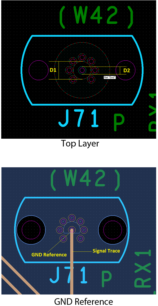
The diameter of the signal via drill hole is 15 mil.
The diameter of the outer GND circle on the top layer is approximately 180 mil.
D1: signal anti-pad = 60 mil diameter.
D2: signal anti-pad = 26 mil diameter.
The GND reference planes for SMA signal routing are extended to the signal via pad to prevent mismatching in this area.
The insertion loss of the connector only is calculated as:
Connector RF Insertion Loss (max) = 0.03 x √f (GHz) dBf is the maximum operating frequency for the channel. For example, for a channel operating at 28 Gbps, the maximum RF insertion loss of an individual SMA connector is 0.12 dB.