A newer version of this document is available. Customers should click here to go to the newest version.
4.1. Identifying Pin Assignments Based on Byte Location
4.2. Assigning the RZQ pin and Dedicated Reference Clock Pin for MIPI D-PHY IP
4.3. Supported I/O Features in MIPI D-PHY I/O Standard
4.4. Using the Remaining I/O Pin from Same Byte Location
4.5. I/O Bank Sharing
4.6. MIPI D-PHY Placement Rules
4.7. MIPI Interface Layout Design Guidelines
4.8. Handling MIPI D-PHY IP Reset
6.2.1.1. IP_ID
6.2.1.2. IP_CAP
6.2.1.3. D0_CAP
6.2.1.4. DN_CAP
6.2.1.5. RX_CAP
6.2.1.6. TX_CAP
6.2.1.7. TX_PREAMBLE_LEN
6.2.1.8. D-PHY_CSR
6.2.1.9. TX_CLK_LANE_PS
6.2.1.10. RX_DLANE_ERR
6.2.1.11. SKEW_CAL_LEN_B0
6.2.1.12. SKEW_CAL_LEN_B1
6.2.1.13. SKEW_CAL_LEN_B2
6.2.1.14. SKEW_CAL_LEN_B3
6.2.1.15. ALT_CAL_LEN_B0
6.2.1.16. ALT_CAL_LEN_B1
6.2.1.17. ALT_CAL_LEN_B2
6.2.1.18. ALT_CAL_LEN_B3
6.2.1.19. CLK_CSR
6.2.1.20. CLK_STATUS
6.2.1.21. DLANE_CSR_0
6.2.1.22. DLANE_STATUS_0
6.2.1.23. RX_DLANE_DESKEW_DELAY_0
6.2.1.24. RX_DLANE_ERR_0
6.2.1.25. DLANE_CSR_1
6.2.1.26. DLANE_STATUS_1
6.2.1.27. RX_DLANE_DESKEW_DELAY_1
6.2.1.28. RX_DLANE_ERR_1
6.2.1.29. DLANE_CSR_2
6.2.1.30. DLANE_STATUS_2
6.2.1.31. RX_DLANE_DESKEW_DELAY_2
6.2.1.32. RX_DLANE_ERR_2
6.2.1.33. DLANE_CSR_3
6.2.1.34. DLANE_STATUS_3
6.2.1.35. RX_DLANE_DESKEW_DELAY_3
6.2.1.36. RX_DLANE_ERR_3
6.2.1.37. DLANE_CSR_4
6.2.1.38. DLANE_STATUS_4
6.2.1.39. RX_DLANE_DESKEW_DELAY_4
6.2.1.40. RX_DLANE_ERR_4
6.2.1.41. DLANE_CSR_5
6.2.1.42. DLANE_STATUS_5
6.2.1.43. RX_DLANE_DESKEW_DELAY_5
6.2.1.44. RX_DLANE_ERR_5
6.2.1.45. DLANE_CSR_6
6.2.1.46. DLANE_STATUS_6
6.2.1.47. RX_DLANE_DESKEW_DELAY_6
6.2.1.48. RX_DLANE_ERR_6
6.2.1.49. DLANE_CSR_7
6.2.1.50. DLANE_STATUS_7
6.2.1.51. RX_DLANE_DESKEW_DELAY_7
6.2.1.52. RX_DLANE_ERR_7
6.2.1.53. TX_LPX
6.2.1.54. TX_HS_EXIT
6.2.1.55. TX_LP_EXIT
6.2.1.56. TX_CLK_PREPARE
6.2.1.57. TX_CLK_ZERO
6.2.1.58. TX_CLK_POST
6.2.1.59. TX_CLK_PRE
6.2.1.60. TX_HS_PREPARE
6.2.1.61. TX_HS_ZERO
6.2.1.62. TX_HS_TRAIL
6.2.1.63. TX_INIT
6.2.1.64. TX_WAKE
6.2.1.65. RX_CLK_LOSS_DETECT
6.2.1.66. RX_CLK_SETTLE
6.2.1.67. RX_HS_SETTLE
6.2.1.68. RX_INIT
6.2.1.69. RX_CLK_POST
6.2.1.70. RX_CAL_REG_CTRL
6.2.1.71. RX_CAL_STATUS_D-PHY
6.2.1.72. RX_CAL_SKEW_W_START_MUX
6.2.1.73. RX_CAL_SKEW_W_END_MUX
6.2.1.74. RX_CAL_ALT_W_START_MUX
6.2.1.75. RX__CAL_ALT_W_END_MUX
6.2.1.76. RX_DESKEW_DELAY_MUX
6.2.1.77. RX_CAL_STATUS_LANE_MUX
6.2.1.78. PRBS_INIT_0
6.2.1.79. PRBS_INIT_1
6.2.1.80. PRBS_INIT_2
6.2.1.81. PRBS_INIT_3
6.2.1.82. PRBS_INIT_4
6.2.1.83. PRBS_INIT_5
6.2.1.84. PRBS_INIT_6
6.2.1.85. TX_TM_CONTROL
6.2.1.86. TX_MNL_IO_0
6.2.1.87. TX_MNL_D_LP_EN
6.2.1.88. RX_TM_CONTROL
6.2.2.1. TG_TOP_CTRL_0
6.2.2.2. TG_TOP_CTRL_1
6.2.2.3. TG_TOP_DONE
6.2.2.4. TG_TOP_FAIL
6.2.2.5. TG_TOP_TEST_EN
6.2.2.6. TG_TOP_TEST_LINK
6.2.2.7. TARGET_TEST_CNT
6.2.2.8. TCHK_CONTROL
6.2.2.9. TCHK_LINK_STATUS
6.2.2.10. HS_DONE_LANES
6.2.2.11. TCHK_LINK_ERR_STATUS
6.2.2.12. LANE_ERROR_SOT_LANES
6.2.2.13. CAL_ERROR_LANES
6.2.2.14. HS_ERR_LANES
6.2.2.15. HS_TEST_CNT
6.2.2.16. LPDT_TEST_CNT
6.2.2.17. TRIGGER_TEST_CNT
6.2.2.18. ULPS_TEST_CNT
6.2.2.19. TG_RX_OVRD_DATA_PAT
6.2.2.20. TG_RX_BIT_ERROR_CNT
6.2.2.21. TG_RX_HS_TXFER_CNT
6.2.2.22. TG_LINK_CONTROL
6.2.2.23. TG_INIT_CNT
6.2.2.24. TG_HS_LEN
6.2.2.25. TG_LP_LEN
6.2.2.26. TG_SKEW_CAL
6.2.2.27. TG_ALT_CAL
6.2.2.28. TG_PER_SKEW_CAL_LEN
6.2.2.29. TG_TEST_CNT
6.2.2.30. TG_OVRD_DATA_PAT
6.2.2.31. TG_TX_HS_TXFER_CNT
5.2. Configuring the D-PHY IP Tab
This topic describes the configuration of the general settings on the D-PHY IP tab in the parameter editor.
Figure 9. D-PHY IP Configuration Tab
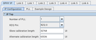
| Parameter Name | Description | Setting |
|---|---|---|
| Number of PLL | Set number of PLL to use for clock generation. The IP can use up to 2 PLLs to share among the different D-PHY links. The bit rates of the D-PHY links has to be the same to share a PLL. | 1 or 2. (Default value is 1.) |
| RZQ Pin | Set RZQ pin location to use for the D-PHY IP. | RZQ0 or RZQ1. (Default value is RZQ0.) Pin 38 in one I/O bank is RZQ0 and pin 62 is RZQ1. Pin 38 reserves BYTE LOCATION 3, and pin 62 reserves BYTE LOCATION 5. |
| Skew calibration length | Length of initial skew calibration pattern automatically generated by D-PHY TX IP when SKEW_CAL_EN = 1. This is done automatically after the t INIT period. When SKEW_CAL_EN = 0, protocol IP is responsible to drive TxSkewCalHS to generate init skew sequence. SKEW_CAL_LEN is ignored by D-PHY RX IP. | 32768 |
| Alternate calibration length | Length of alternate calibration pattern automatically generated by D-PHY TX IP when ALT_CAL_EN = 1. This is done automatically after the init skew. When SKEW_CAL_EN = 0, protocol IP is responsible to drive TxAlTCalHS to generate alt cal sequence.ALT_CAL_LEN is ignored by D-PHY RX IP. | 65536 |
D-PHY IP PLL Tab
On the PLL tab, you configure the PLL settings such as core clock divider, PLL reference clock frequency, I/O standard selection, and VCO clock frequency.
Figure 10. D-PHY IP PLL Tab
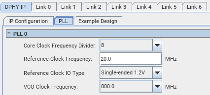
| Parameter Name | Description | Setting |
|---|---|---|
| Core clock frequency divider | Set core clock frequency divider to generate core clock from VCO output. MIPI only supports divided by 4 or 8. | 4 or 8. (Default value is 8.) |
| Reference clock frequency | PLL reference clock frequency. | 10MHz - 300MHz. (Default value is 20MHz.) |
| Reference clock I/O type | Reference Clock I/O standard. | Single Ended 1.2V, LVDS 1.2V Single Ended 1.1V, LVDS 1.1V . |
| Share Reference Clock I/O | Enable PLL1 share reference clock with PLL0. | True or False. (Default value is True.) |
| VCO Clock Frequency | Sets the VCO clock frequency for PLL. - MIPI TX with bitrate > 1.2Gbps: VCO freq = 1/2 bit rate. - MIPI TX with bitrate 1.2Gbps: VCO freq = 1/2 bitrate * Tx bitrate divider (1, 2, 4 of 8). - MIPI RX with skew calibration disabled: no dependency between VCO freq and bit rate. -MIPI RX with skew calibration enabled: VCO freq = 1/2 bitrate |
600MHz - 1740MHz. |