AN 669: Drive-On-Chip Design Example for Cyclone V Devices
ID
683466
Date
5/15/2022
Public
1. About the Drive-On-Chip Design Example for Cyclone V Devices
2. Motor Control Boards
3. Drive-On-Chip Design Example for Cyclone V Devices Features
4. Getting Started
5. Building the Design
6. Debugging and Monitoring the Drive-On-Chip Design Example with System Console
7. About the Scaling of Feedback Signals
8. Motor Control Software
9. Functional Description of the Drive-On-Chip Design Example
10. Achieving Timing Closure on a Motor Control Design
11. Design Security Recommendations
12. Reference Documents for the Drive-on-Chip Design Example
13. Document Revision History for AN 669: Drive-on-Chip Reference Design
4.1. Software Requirements for the Drive-On-Chip Design Example for Cyclone V Devices
4.2. Downloading and Installing the Drive-On-Chip Design Example for Cyclone V Devices
4.3. Setting Up the Motor Control Board with your Development Board
4.4. Programming the Hardware onto the Device
4.5. Setting Up Terminal Emulator
4.6. Downloading the HPS Software to the Device
6.1. System Console GUI Upper Pane for the Drive-On-Chip Design Example
6.2. System Console GUI Lower Pane for the Drive-On-Chip Design Example
6.3. Vibration Suppression Tab
6.4. Controlling the DC-DC Converter
6.5. Tuning the PI Controller Gains
6.6. Controlling the Speed and Position Demonstrations
6.7. Monitoring Performance
9.1. Processor Subsystem
9.2. Six-channel PWM Interface
9.3. DC Link Monitor
9.4. Drive System Monitor
9.5. Quadrature Encoder Interface
9.6. Sigma-Delta ADC Interface for Drive Axes
9.7. DC-DC Converter
9.8. Motor Control Modes
9.9. FOC Subsystem
9.10. FFTs
9.11. DEKF Technique for Battery Management
9.12. Signals
9.13. Registers
9.9.1. DSP Builder for Intel FPGAs Model for the Drive-On-Chip Designs
9.9.2. Avalon Memory-Mapped Interface
9.9.3. About DSP Builder for Intel FPGAs
9.9.4. DSP Builder for Intel FPGAs Folding
9.9.5. DSP Builder for Intel FPGAs Model Resource Usage
9.9.6. DSP Builder for Intel FPGAs Design Guidelines
9.9.7. Generating VHDL for the DSP Builder Models for the Drive-On-Chip Reference Designs
Downloading and Installing the Reference Design
- Download the relevant reference design .par file for your development kit and power board from the Intel Design Store.
To obtain further support on the reference design, contact your local Intel sales representative.
- Install the relevant reference design .par file for your development kit and power board.
Table 3. Design .par Files Variant Development Kit Power Board Processor DOC_4AXIS_CVSX Cyclone V SoC Intel 4 Axis HPS DOC_FE2H_CVSX Cyclone V SoC FalconEye 2 HSMC HPS DOC_FE2H_CVSX_XiP Cyclone V SoC FalconEye 2 HSMC HPS DOC_FE2H_MAX10 MAX 10 FPGA FalconEye 2 HSMC Nios II DOC_FE2H_SoCKit SoCKit FalconEye 2 HSMC HPS Note: The XiP variant does not use external DDR3 memory and executes all code directly from flash memory. - In the Quartus II software, click File > New Project Wizard.
- Click Next.
- Enter the path for your project working directory and enter variant name from the table for the project name.
- Click Next.
- Select Project Template.
- Click Next
- Click Install the design templates.
- Browse to select the .par file for the reference design and browse to the destination directory where you want to install it.
Figure 1. Design Template Installation
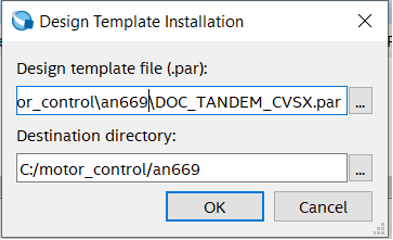
- Click OK on the design template installation message.
- Select the Drive on Chip Reference design design example.
Figure 2. Design Template
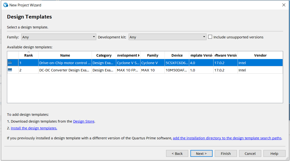
- Click Next.
- Click Finish. The Quartus II software expands the archive and sets up the project, which may take some time.
Figure 3. Directory StructureThe reference design directory structure for the DOC_FE2H_CVSX variant
Related Information