AN 669: Drive-On-Chip Design Example for Cyclone V Devices
ID
683466
Date
5/15/2022
Public
1. About the Drive-On-Chip Design Example for Cyclone V Devices
2. Motor Control Boards
3. Drive-On-Chip Design Example for Cyclone V Devices Features
4. Getting Started
5. Building the Design
6. Debugging and Monitoring the Drive-On-Chip Design Example with System Console
7. About the Scaling of Feedback Signals
8. Motor Control Software
9. Functional Description of the Drive-On-Chip Design Example
10. Achieving Timing Closure on a Motor Control Design
11. Design Security Recommendations
12. Reference Documents for the Drive-on-Chip Design Example
13. Document Revision History for AN 669: Drive-on-Chip Reference Design
4.1. Software Requirements for the Drive-On-Chip Design Example for Cyclone V Devices
4.2. Downloading and Installing the Drive-On-Chip Design Example for Cyclone V Devices
4.3. Setting Up the Motor Control Board with your Development Board
4.4. Programming the Hardware onto the Device
4.5. Setting Up Terminal Emulator
4.6. Downloading the HPS Software to the Device
6.1. System Console GUI Upper Pane for the Drive-On-Chip Design Example
6.2. System Console GUI Lower Pane for the Drive-On-Chip Design Example
6.3. Vibration Suppression Tab
6.4. Controlling the DC-DC Converter
6.5. Tuning the PI Controller Gains
6.6. Controlling the Speed and Position Demonstrations
6.7. Monitoring Performance
9.1. Processor Subsystem
9.2. Six-channel PWM Interface
9.3. DC Link Monitor
9.4. Drive System Monitor
9.5. Quadrature Encoder Interface
9.6. Sigma-Delta ADC Interface for Drive Axes
9.7. DC-DC Converter
9.8. Motor Control Modes
9.9. FOC Subsystem
9.10. FFTs
9.11. DEKF Technique for Battery Management
9.12. Signals
9.13. Registers
9.9.1. DSP Builder for Intel FPGAs Model for the Drive-On-Chip Designs
9.9.2. Avalon Memory-Mapped Interface
9.9.3. About DSP Builder for Intel FPGAs
9.9.4. DSP Builder for Intel FPGAs Folding
9.9.5. DSP Builder for Intel FPGAs Model Resource Usage
9.9.6. DSP Builder for Intel FPGAs Design Guidelines
9.9.7. Generating VHDL for the DSP Builder Models for the Drive-On-Chip Reference Designs
10. Achieving Timing Closure on a Motor Control Design
Intel® Quartus® Prime may not achieve full timing closure when it first compiles and fits this designs.
You must assume worst-case timing parameters over a wide range of temperature, which is good practice for a commercial design. If you run this design at room temperature, it is unlikely that real timing violations occur. To achieve full timing closure with Intel® Quartus® Prime, you may include additional pipeline registers. However, the place-and-route process is sensitive to an initial seed value and the result of different seeds is not easy to predict. Before optimizing the design, try the seed sweep function with many different seed values in case the design immediately fits.
- In Intel® Quartus® Prime, select Tools > Launch Design Space Explorer II.
Design space Explorer opens in a seaparate window.
- For a basic seed sweep use the following settings:
- In Setup, select Local.
- In Exploration, select Design exploration, exploration mode: Seed Sweep Only, create 10 seeds.
- Click Start to run.
Figure 53. Exploration windowUse Results to view when all are finished
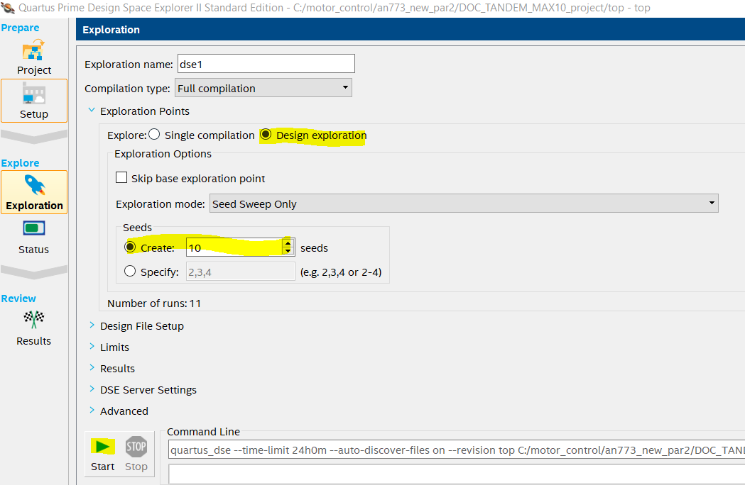 Figure 54. Result window
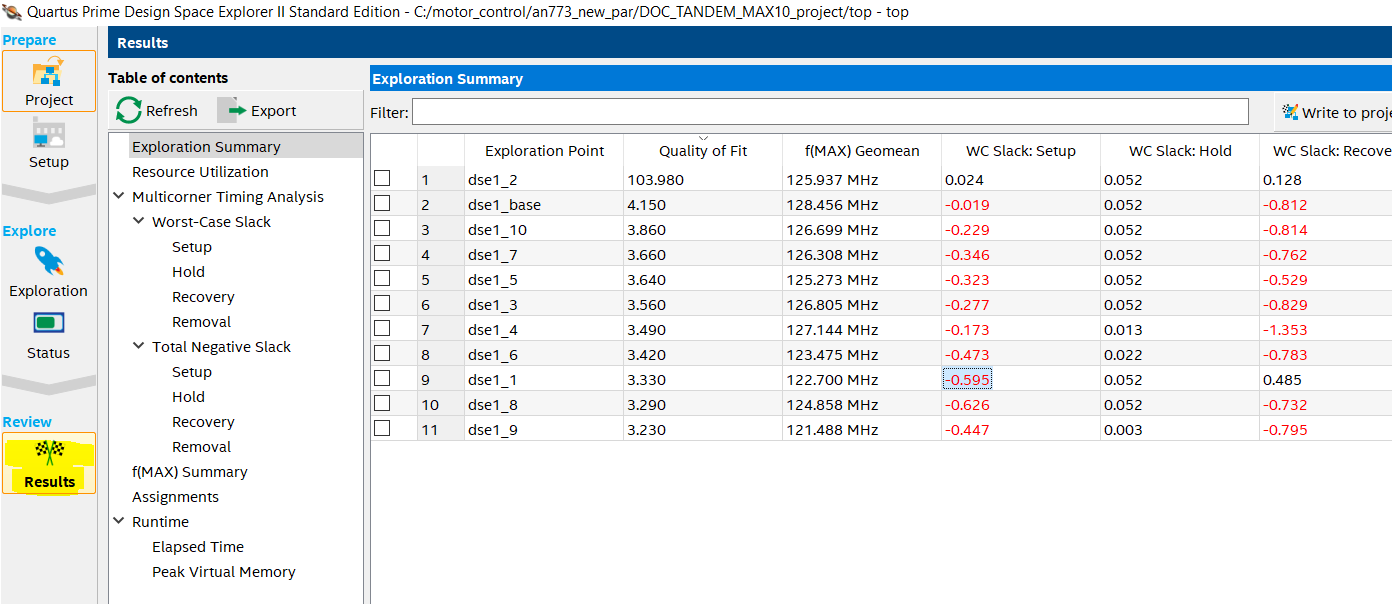
- Calculate the seed number from the exploration point name. It is the _number plus 1. In this example, the best seed will be 2(dse1_2) + 1 = 3.
- Select Assignments > Settings.
- In complier settings, click Advanced settings (Fitter)….
- Update seed value Fitter Initial Placement Seed 3.