ALTDQ_DQS2 Features


                                ALTDQ_DQS2 Device Support


                                Resource Utilization and Performance


                                ALTDQ_DQS2 Parameter Settings


                                ALTDQ_DQS2 Data Paths


                                ALTDQ_DQS2 Ports


                                Dynamic Reconfiguration for ALTDQ_DQS2


                                Stratix V Design Example


                                Arria V Design Example


                                IP-Generate Command


                                ALTDQ_DQS2 IP Core User Guide Archives


                                Document Revision History


                                            I/O Configuration Block Bit Sequence for Arria V GZ and Stratix V Devices


                                            DQS Configuration Block Bit Sequence for Arria V GZ and Stratix V Devices


                                            I/O Configuration Block Bit Sequence for Arria V and Cyclone V Devices


                                            DQS Configuration Block Bit Sequence for Arria V and Cyclone V Devices


                                            Example Usage of Dynamic Reconfiguration for ALTDQ_DQS2


                            SDC Walkthrough
To create a new .sdc, follow these steps:
-   Constrain the clocks coming into the FPGA with the create_clock command. The following command creates the base clock for the input clock port driving the PLL:  
    create_clock -name refclk -period 10.000 [get_ports {refclk}]
 -  Create the generated clocks for the PLL with the following command: 
    derive_pll_clocks
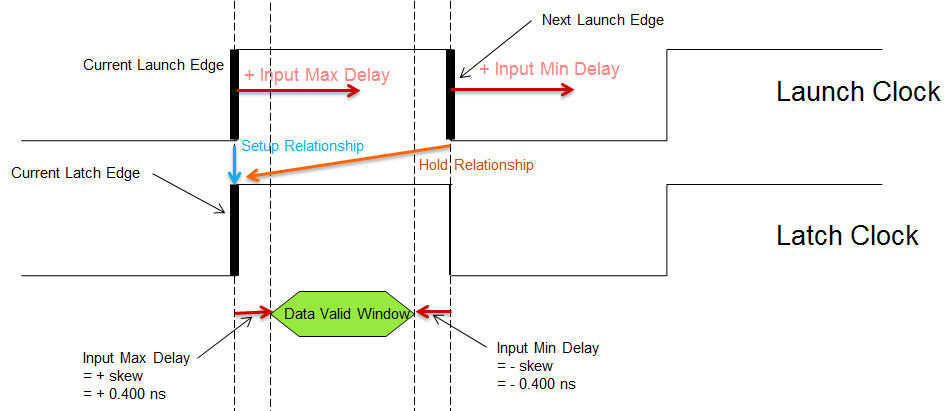
 -   Constraint the virtual input clock (for incoming DQS strobe) and the strobe_in port. ln this design example, it is based on a 200 MHz input clock, with a 50% duty cycle, where the first rising edge occurs at 0 ns. 
    
create_clock -name virtual_dqs_in -period 5.000
create_clock -name dqs_in -period 5.000[get_ports {strobe_in}]
 -   lncoming data is edge-aligned to the DQS strobe, and the minimum and maximum input delay is assumed to be ± 0.4 ns in this design example. You must modify constraints to reflect the data and clock relationship in the system. Use the -add option to add the your delay constraint instead of overriding previous constraints. 
    set_input_delay -clock {virtual_dqs_in} -max -add_delay 0.400 [get_ports {read_write_data_io[*]}]
set_input_delay -clock {virtual_dqs_in} -min -add_delay -0.400 [get_ports{read_write_data_io[*]}]
set_input_delay -clock {virtual_dqs_in} -clock_fall -max -add_delay 0.400 [get_ports {read_write_data_io[*]}]
set_input_delay -clock {virtual_dqs_in} -clock_fall -min -add_delay -0.400 [get_ports {read_write_data_data_io[*]}]
Figure 43. Input Delay Timing Analysis