ALTDQ_DQS2 Features
ALTDQ_DQS2 Device Support
Resource Utilization and Performance
ALTDQ_DQS2 Parameter Settings
ALTDQ_DQS2 Data Paths
ALTDQ_DQS2 Ports
Dynamic Reconfiguration for ALTDQ_DQS2
Stratix V Design Example
Arria V Design Example
IP-Generate Command
ALTDQ_DQS2 IP Core User Guide Archives
Document Revision History
I/O Configuration Block Bit Sequence for Arria V GZ and Stratix V Devices
DQS Configuration Block Bit Sequence for Arria V GZ and Stratix V Devices
I/O Configuration Block Bit Sequence for Arria V and Cyclone V Devices
DQS Configuration Block Bit Sequence for Arria V and Cyclone V Devices
Example Usage of Dynamic Reconfiguration for ALTDQ_DQS2
Understanding Simulation Results—Arria V Design Example
ln the Arria V design example, a generic testbench is used to test the write and read operations in the ALTDQ_DQS2 IP core. The following table lists the components in the testbench.
| Component | Description |
|---|---|
| DQS Driver |
|
| DQS Agent |
|
Note: Random data is generated and used in the testbench. You may see other data values if you are using different operating system and seeds.
The following figure shows the waveform for the testbench generated after executing the top_run_msim_rtl_verilog.do file.
Figure 38. Example Waveform
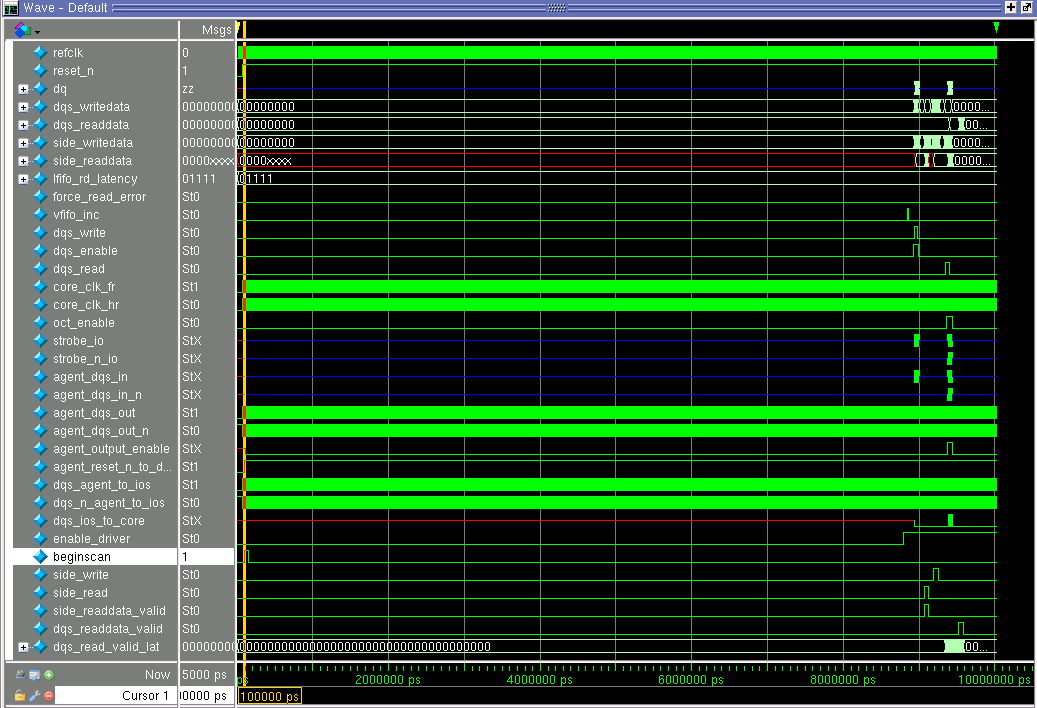
All ports are in reset mode until the reset_n signal is asserted at 70 ns. Then, the core_clk_fr and core_clk_hr clocks start to toggle. The agent_reset_n_to_dqs signal is asserted at 95 ns to reset the ALTDQ_DQS2 IP core located in top_inst.