ALTDQ_DQS2 Features
ALTDQ_DQS2 Device Support
Resource Utilization and Performance
ALTDQ_DQS2 Parameter Settings
ALTDQ_DQS2 Data Paths
ALTDQ_DQS2 Ports
Dynamic Reconfiguration for ALTDQ_DQS2
Stratix V Design Example
Arria V Design Example
IP-Generate Command
ALTDQ_DQS2 IP Core User Guide Archives
Document Revision History
I/O Configuration Block Bit Sequence for Arria V GZ and Stratix V Devices
DQS Configuration Block Bit Sequence for Arria V GZ and Stratix V Devices
I/O Configuration Block Bit Sequence for Arria V and Cyclone V Devices
DQS Configuration Block Bit Sequence for Arria V and Cyclone V Devices
Example Usage of Dynamic Reconfiguration for ALTDQ_DQS2
Understanding Simulation Results—Stratix V Design Example
ln the Stratix V design example, a generic testbench is used to test the write and read operations in the ALTDQ_DQS2 IP core. The following table lists the components in the testbench.
| Component | Description |
|---|---|
| DQS Driver |
|
| DQS Agent |
|
Note: Random data is generated and used in the testbench. You may see other data values if you are using a different operating system and seeds.
The following figure shows the waveform for the testbench generated after executing the top_run_msim_rtl_verilog.do file.
Figure 19. Waveform Example
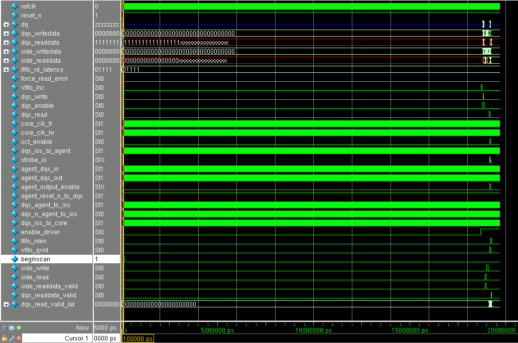
All ports are in reset mode until the reset_n signal is asserted at 70 ns. Then, the core_clk_fr and core_clk_hr clocks start to toggle. The agent_reset_n_to_dqs signal is asserted at 91 ns to reset the ALTDQ_DQS2 IP core, which is located in top_inst.