ALTDQ_DQS2 Features
ALTDQ_DQS2 Device Support
Resource Utilization and Performance
ALTDQ_DQS2 Parameter Settings
ALTDQ_DQS2 Data Paths
ALTDQ_DQS2 Ports
Dynamic Reconfiguration for ALTDQ_DQS2
Stratix V Design Example
Arria V Design Example
IP-Generate Command
ALTDQ_DQS2 IP Core User Guide Archives
Document Revision History
I/O Configuration Block Bit Sequence for Arria V GZ and Stratix V Devices
DQS Configuration Block Bit Sequence for Arria V GZ and Stratix V Devices
I/O Configuration Block Bit Sequence for Arria V and Cyclone V Devices
DQS Configuration Block Bit Sequence for Arria V and Cyclone V Devices
Example Usage of Dynamic Reconfiguration for ALTDQ_DQS2
DQS Delay Chain
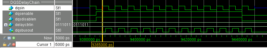
The dqsenable signal grounds the DQS input strobe after the strobe goes to Hi-Z. This is important for bidirectional strobes, where glitches can be filtered effectively through the DQS enable. The dqsbusout signal is the delayed dqsin signal that drives into the dedicated DQS clock network to clock the DQ capture registers so that data is captured at the centre of the eye. The following figure shows a 90° phase shift between the dqsin and dqsbusout signals. This is consistent with the settings in Instantiating the ALTDQ_DQS2 IP Core.
Figure 40. DQS Delay Chain Waveform