ALTDQ_DQS2 Features
ALTDQ_DQS2 Device Support
Resource Utilization and Performance
ALTDQ_DQS2 Parameter Settings
ALTDQ_DQS2 Data Paths
ALTDQ_DQS2 Ports
Dynamic Reconfiguration for ALTDQ_DQS2
Stratix V Design Example
Arria V Design Example
IP-Generate Command
ALTDQ_DQS2 IP Core User Guide Archives
Document Revision History
I/O Configuration Block Bit Sequence for Arria V GZ and Stratix V Devices
DQS Configuration Block Bit Sequence for Arria V GZ and Stratix V Devices
I/O Configuration Block Bit Sequence for Arria V and Cyclone V Devices
DQS Configuration Block Bit Sequence for Arria V and Cyclone V Devices
Example Usage of Dynamic Reconfiguration for ALTDQ_DQS2
Setting Up NativeLink and Simulation Settings
To set up the NativeLink and simulation settings, follow these steps:
- In the Quartus® Prime software, on the Tools menu, select Options.
- In the Options dialog box, under Category list, expand General and then select EDA Tool Options.
- In the EDA Tools Options window, follow the settings as shown in the following figure:
Figure 14. EDA Tools Options Dialog Box

- In the Quartus® Prime software, on the Assignments menu, click Settings > Simulation.
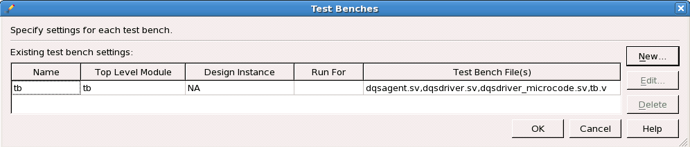
- Create a new testbench and name it tb and include all necessary files.
- Enter the necessary NativeLink settings. The following figure shows an example settings.
Figure 15. Simulation Dialog Box
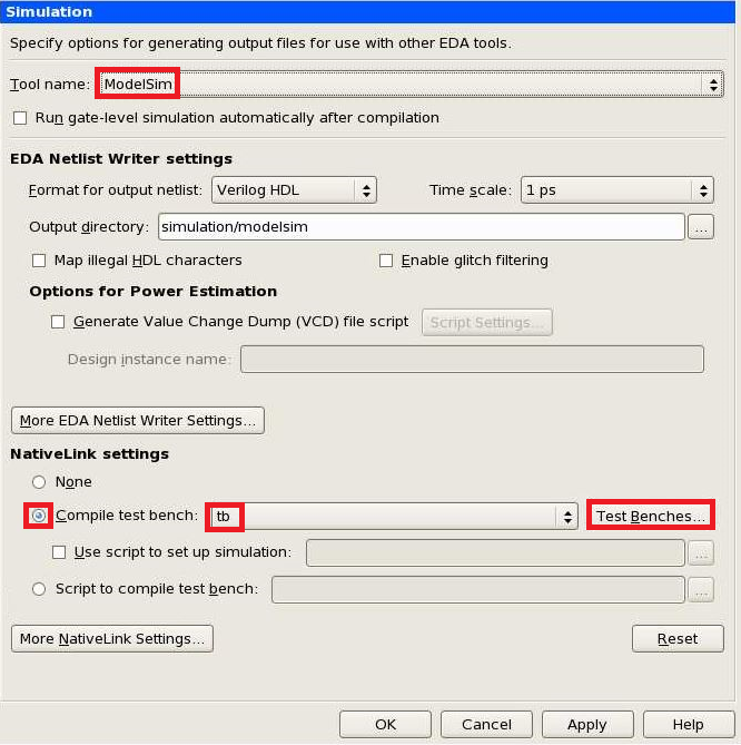
Figure 16. Test Benches Dialog Box
- Run Analysis and Synthesis.
- To view the simulation results, on the Tools menu, select Run Simulation Tool and then click RTL Simulation.
For a successful simulation, you may need to manually change alterapll.vo to alterapll.v in the auto-generated top_run_msim_rtl_verilog.do file.
- Before running the Fitter, ensure that the following settings are done in the Assignment Editor.
- I/O Standard
- Input Termination
- Output Termination
- DQ Group
- Location assignment for strobe pin—this helps the Fitter to fit the related DQ pins in the appropriate l/O sub-banks. You can then back-annotate the locations if desired.
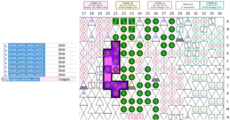
The following figures show a setting example in the Assignment Editor and the Pin Planner result:Figure 17. Setting Example in Assignment Editor
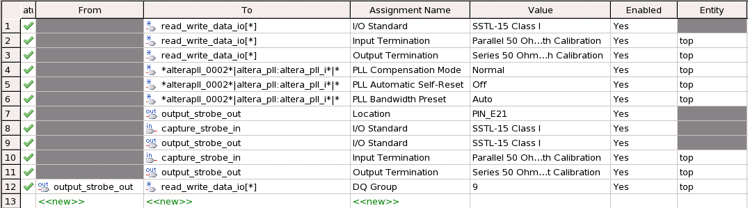
Figure 18. Pin Planner
- Run the Fitter, Timing Analysis, and Assembler. Refer to SDC Walkthrough for more elaboration on the SDC constraint examples included in this design example.
Related Information