25G Ethernet Intel® Stratix® 10 FPGA IP Design Example User Guide
ID
683252
Date
6/18/2020
Public
A newer version of this document is available. Customers should click here to go to the newest version.
1. 25G Ethernet Intel® FPGA IP Quick Start Guide
2. 10G/25G Ethernet Single-Channel Design Example for Intel® Stratix® 10 Devices
3. 25G Ethernet Single-Channel Design Example for Intel® Stratix® 10 Devices
4. 25G Ethernet Multi-Channel Design Example for Intel Stratix 10 Devices
5. 25G Ethernet Intel® FPGA IP Design Example References
6. 25G Ethernet Intel® Stratix® 10 FPGA IP Design Example User Guide Archives
7. Document Revision History for the 25G Ethernet Intel® Stratix® 10 FPGA IP Design Example User Guide
1.1. Directory Structure
1.2. Generating the Design Example
1.3. Simulating the 25G Ethernet Intel® FPGA IP Design Example Testbench
1.4. Compiling and Configuring the Design Example in Hardware
1.5. Changing Target Device in Hardware Design Example
1.6. Testing the 25G Ethernet Intel® FPGA IP Design in Hardware
3.4.3. Test Case—Design Example Without the IEEE 1588v2 Feature
The simulation test case performs the following actions:
- Instantiates and ATX PLL.
- Waits for RX clock and PHY status signal to settle.
- Prints PHY status.
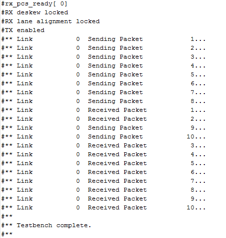
- Analyzes the results. The successful testbench sends ten packets, receives ten packets, and displays "Testbench complete."
Figure 18. Sample Simulation Output for Design Example Without the IEEE 1588v2 Feature