A newer version of this document is available. Customers should click here to go to the newest version.
1.4.3.3. Performing PFL Simulation for FPGA Configuration
In this simulation example, the start and end addresses of the option bits sector are 0×800000 and 0×800080, respectively. The PFL IP core first reads from the final address, which is 0×800080, to obtain the .pof version information. Because fpga_pgm[2..0] is set to 000, the PFL IP core reads from address 0×800000 to address 0×800003 to get the start and end address of page 0 and the Page-Valid bit. The LSB in address 0×800000 is the Page-Valid bit.
The Page-Valid bit must be 0 for the PFL IP core to proceed with FPGA configuration. While the PFL IP core reads from the flash, it asserts the active-low flash_nce and flash_noe signals, and asserts the active-high pfl_flash_access_request signal.
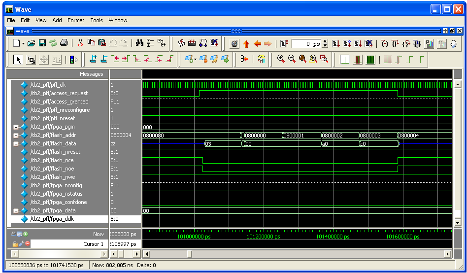
After reading the option bits for page 0, the PFL IP core waits for a period of time before the configuration starts. The flash_data remains at 0×ZZ within this period. Configuration starts when the fpga_dclk starts to toggle. During configuration, the PFL IP core asserts the flash_nce and flash_noe signals low, and the pfl_flash_access_request signal high.
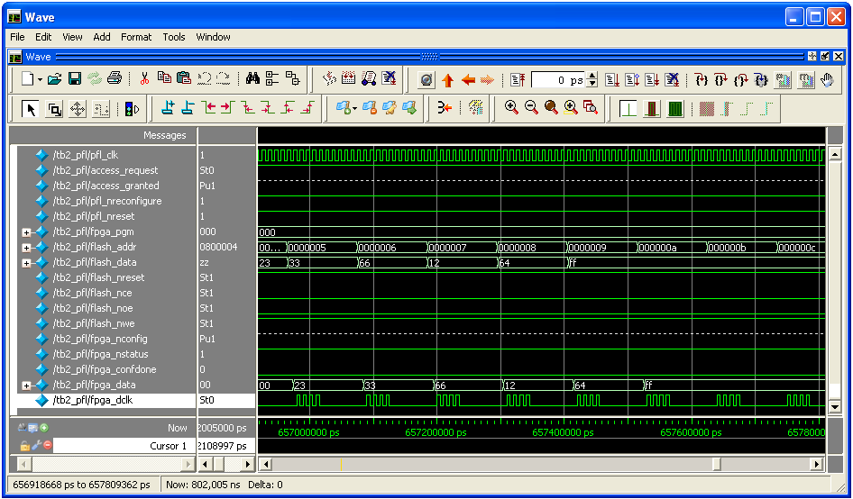
The FPGA configuration continues until the fpga_conf_done signal is asserted high, which indicates the configuration is complete. After the configuration process completes, the PFL IP core pulls the flash_nce and flash_noe signals high and the pfl_flash_access_request signal low to indicate the configuration data is no longer being read from the flash memory device.