A newer version of this document is available. Customers should click here to go to the newest version.
1.1. Features
1.2. Device Support
1.3. Functional Description
1.4. Using the PFL IP Core
1.5. PFL IP Core In Embedded Systems
1.6. Third-party Programmer Support
1.7. Parameters
1.8. Signals
1.9. Specifications
1.10. Parallel Flash Loader Intel® FPGA IP User Guide Archives
1.11. Document Revision History for the Parallel Flash Loader Intel® FPGA IP User Guide
1.4.1. Converting .sof Files to a .pof
1.4.2. Constraining PFL Timing
1.4.3. Simulating PFL Design
1.4.4. Programming Intel® CPLDs and Flash Memory Devices
1.4.5. Defining New CFI Flash Device
1.4.6. Programming Multiple Flash Memory Devices
1.4.7. Creating Jam Files for Intel® CPLDs and Flash Memory Device Programming
1.3.1. Programming Flash Memory
You can use the PFL IP to program the following flash memory devices with JTAG interface:
- Programming CFI Flash
- Programming Quad SPI Flash
- Programming NAND Flash
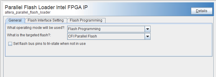
Figure 1. Parallel Flash Loader Intel® FPGA IP Parameter EditorFigure shows the General tab of the Parallel Flash Loader Intel® FPGA IP parameter editor.