DSP Builder for Intel® FPGAs (Advanced Blockset): Handbook
A newer version of this document is available. Customers should click here to go to the newest version.
7.9. DSP Builder HDL Import Design Example
The digital upconverter includes: input memory, upconverter, FIR filter, scaler, mixer and digital predistortion (DPD).
| hdl_import_duc.mdl | The DSP Builder design. |
| hdl_import_duc_params.xml | The design's parameter file. |
| hdl_import_calc_fir_coefs.m | A script to generate the FIR coefficients using MATLAB's cfirpm function. DSP Builder prints the coefficients to MATLAB's Command Window and you can copy and paste them into coefficients.vhd. |
| calc_dpd_coefs.m | A script to generate the DPD coefficients using a simple polynomial model of a power amplifier. DSP Builder prints the coefficients MATLAB's Command Window and you can copy and paste them into lut_dpd.vhd. |
| to_import | This directory contains 12 VHDL source files. |
VHDL Components
The design example includes a complex FIR filter in VHDL optimized for Intel Stratix 10 devices. This FIR filter has one valid data sample every eight clock cycles.
See Designing Filters for High Performance.The simple LUT-based DPD is initialized with a third-order polynomial.
Top-Level Design
The top-level design contains the device-level subsystem and five downsample and spectrum analyzer blocks from MathWork's DSP System Toolbox. These blocks show the spectral output from the various stages of the up-conversion chain.
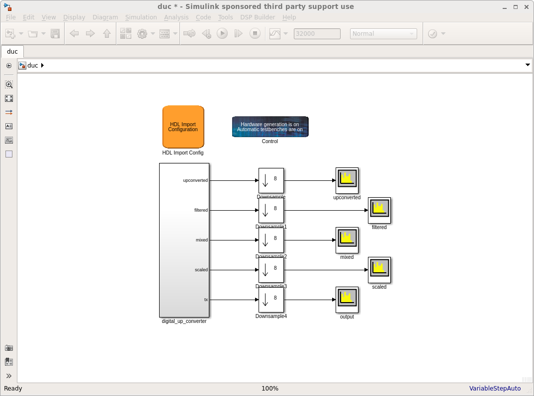
Digital Up Converter
The digital_up_converter subsystem is the device-level subsystem. It contains all of the design's DSP Builder-based components and two gaps for HDL Import blocks.

Buffer and Upsample
This scheduled subsystem contains two SharedMem blocks, which contain the 20 MSPS baseband source: one for the real part of the signal and one for the imaginary part. You can write to the blocks via the bus or use the preloaded tones.
The read_counter block drives the upconversion. It counts modulo 32 because it upsamples the 20 MSPS baseband by 4 to 80 MSPS and then holds each sample for 8 clock cycles at a clock rate of 640 MHz. The FIR filter accepts one sample every eight cycles. By holding the samples, the FIR does not need synchronization logic.

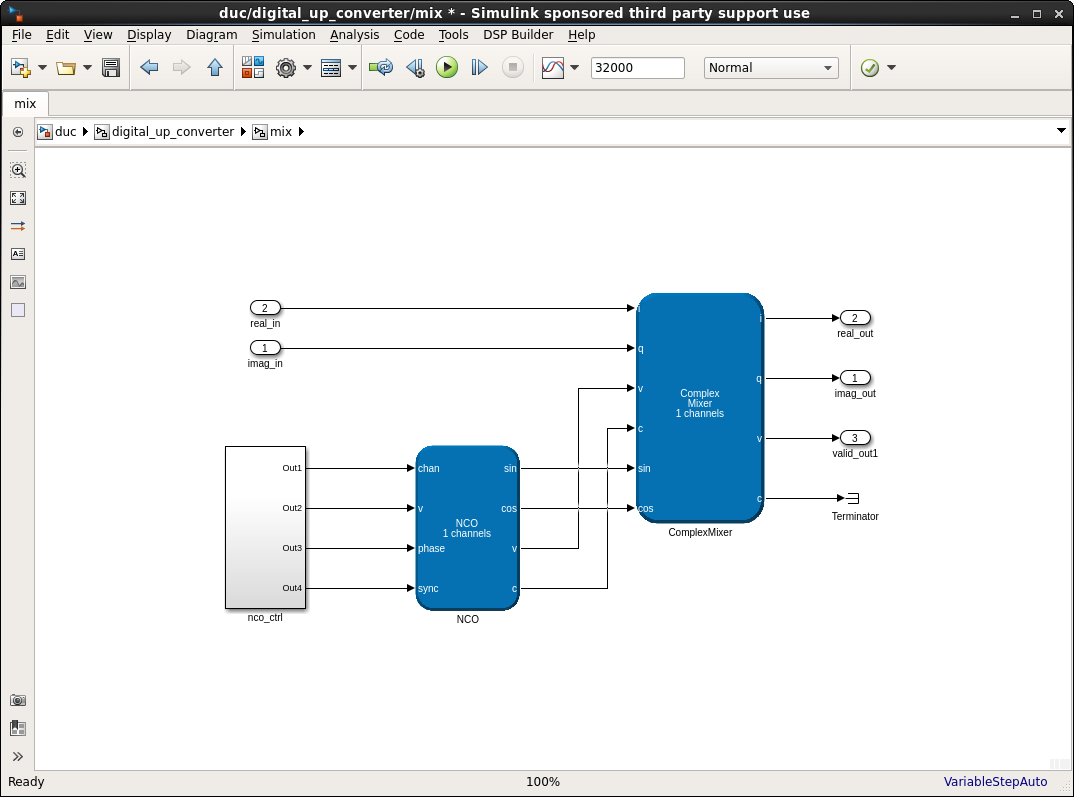
Mixer
This single-channel mixer consists of NCO and ComplexMixer IP blocks and a scheduled subsystem for controlling the NCO. The control subsystem asserts the valid signal once every eight cycles. The NCO generates a 16 MHz complex tone, which the ComplexMixer uses to mix the filtered signal.
Scale
The scale scheduled subsystem scales the data so that it fits within the DPD's range of operation by bit-shifting from the mixer's output. You can use the optional multiplier for increasing the signal level if bit-shifting is insufficient.

FIR Coefficients
The FIR coefficients are defined in coefficients.vhd.
The coefficients are calculated in hdl_import_calc_fir_coefs.m. This script uses MATLAB’s cfirpm command to create complex coefficients.
DPD
The file lut_dpd.vhd contains the DPD for this design example. The DPD consists of an address generator that indexes a LUT. The output of the LUT is then multiplied with the complex input data. The LUT contents are calculated in hdl_import_calc_dpd_coefs.m. This script uses a simple, real-numbered, third-order model of an amplifier to calculate predistortion coefficients. DSP Builder uses these coefficients to calculate the LUT contents.
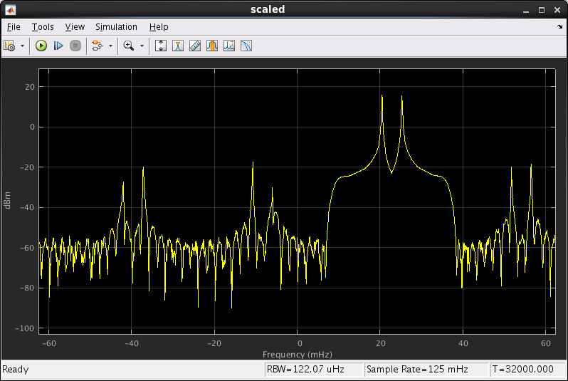
Simulink Simulations Results
The first four waveforms are the real and imaginary input and output of the FIR. The FIR smooths the zero-padded signals.
The next four waveforms are the real and imaginary input and output of the the DPD.

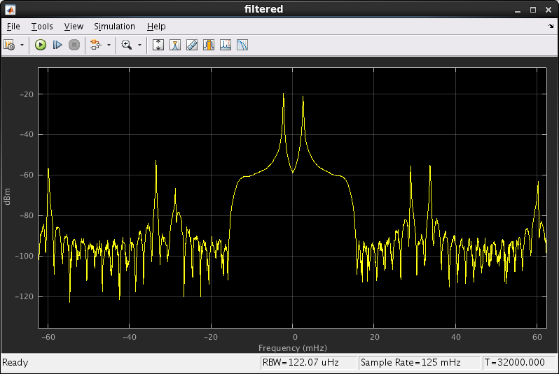
The two preloaded memory signals are clearly visible about 0, as are their four aliases because of the zero-insert upsampling.

The aliased signals are attenuated by 40dB, as expected from the analysis in calc_fir_coefs.m.
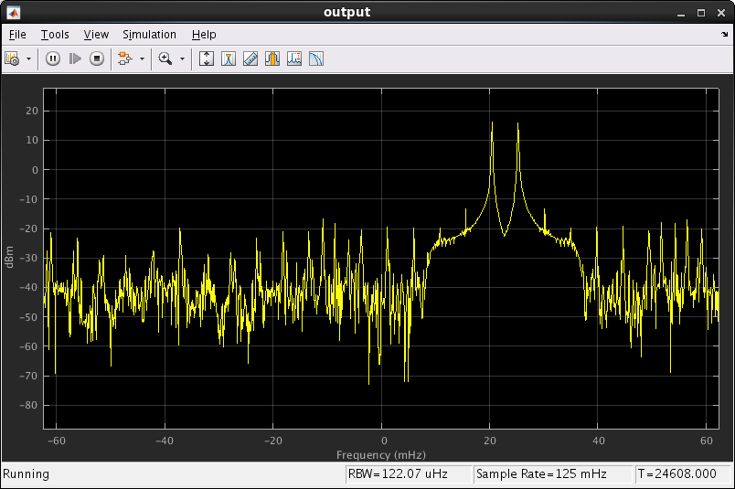
The mixed spectrum shows the baseband signal moving over to be centered on 16 MHz. This view shows the Simulink clock rate of 1 Hz rather than the FPGA clock rate of 640 MHz, so 16 MHz becomes 25 mHz.

Scaled looks identical to mixed, except that the signal amplitude is much greater.
The post-DPD output signal is a noiser version of the scaled signal. Observe the two third-order harmonics in the pass-band.