DSP Builder for Intel® FPGAs (Advanced Blockset): Handbook
A newer version of this document is available. Customers should click here to go to the newest version.
7.3. DSP Builder DDC Design Example
Intermediate frequency (IF) modem designs have multichannel, multirate filter lineups. The filter lineup is often programmable from a host processor, and has stringent demands on DSP performance and accuracy.The DDC design example is a high-performance design running at over 350 MHz in an Intel Arria 10 device. The design example is very efficient and at under 4,000 logic registers gives a low cost per channel.
View the DDCChip subsystem to see the components you require to build a complex, production ready system.
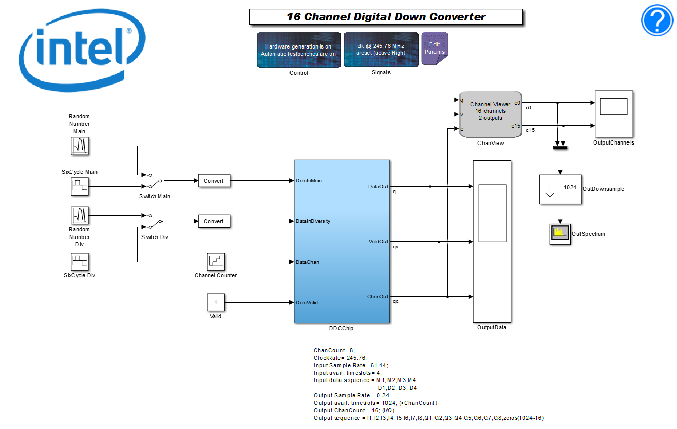
The top-level testbench includes Control and Signals blocks, and some Simulink blocks to generate source signals and visualize the output. The full power of the Simulink blocksets is available for your design.
The DDCChip subsystem block contains the following blocks that form the lowest level of the design hierarchy:
- The NCO and mixer
- Decimate by 16 CIC filter
- Two decimate by 4 FIR odd-symmetric filters: one with length 21, the other length with 63.
The other blocks in this subsystem perform a range of rounding and saturation functions. They also allow dynamic scaling. The Device block specifies the target FPGA.
DDC Signals Block
The Signals block allows you to define the relationship between the sample rates and the system clock, to tell the synthesis engines how much folding or time sharing to perform. Increasing the system clock permits more folding, and therefore typically results in more resource sharing, and a smaller design.
You also need a system clock rate so that the synthesis engines know how much to pipeline the logic. For example, by considering the device and speed grade, the synthesis tool can calculate the maximum length that an adder can have. If the design exceeds this length, it pipelines the adder and adjusts the whole pipeline to compensate. This adjustment typically results in a small increase in logic size, which is usually more than compensated for by the decrease in logic size through increased folding.
The Signals block specifies the clock and reset names, with the system clock frequency. The bus clock or FPGA internal clock for the memory-mapped interfaces can be run at a lower clock frequency. This lets the design move the low-speed operations such as coefficient update completely off the critical path.
DDC Control Block
The Control block controls the whole DSP Builder advanced blockset environment. It examines every block in the system, controls the synthesis flow, and writes out all RTL and scripts. A single control block must be present in every top-level model.
In this design, hardware generation creates RTL. DSP Builder places the RTL and associated scripts in the directory ../rtl, which is a relative path based on the current MATLAB directory. DSP Builder creates automatic self-checking testbenches, which saves the data that a Simulink simulation captures to build testbench stimulus for each block in your design. DSP Builder generates scripts to run these simulations.
The threshold values control the hardware generation. They control the trade-offs between hardware resources, such as hard DSP blocks or soft LE implementations of multipliers. You can perform resource balancing for your particular design needs with a few top-level controls.
DDC Memory Maps
Many memory-mapped registers in the design exist such as filter coefficients and control registers for gains. You can access these registers through a memory port that DSP Builder automatically creates at the top-level of your design. DSP Builder can create all address decode and data multiplexing logic automatically. DSP Builder generates a memory map in XML and HTML that you can use to understand the design.
To access this memory map, after simulation, on the DSP Builder menu, point to Resource Usage and click Design, Current Subsystem, or Selected block. The address and data widths are set to 8 and 32 in the design.
DDC EditParams Blocks
The EditParams block allows you to edit the script setup_demo_ddc.m, which sets up the MATLAB variables that configure your model. Use the MATLAB design example properties callback mechanism to call this script.
You can edit the parameters in the setup_demo_ddc.m script by double-clicking on the Edit Params block to open the script in the MATLAB text editor.
The script sets up MATLAB workspace variables. The SampleRate variable is set to 61.44 MHz, which typical of a CDMA system, and represents a quarter of the system clock rate that the FPGA runs at. You can use the feature to TDM four signals onto any given wire.
DDC Source Blocks
The Simulink environment enables you to create any required input data for your design. In the DDC design, use manual switches to select sine wave or random noise generators. DSP Builder encodes a simple six-cycle sine wave as a table in a Repeating Sequence Stair block from the Simulink Sources library. This sine wave is set to a frequency that is close to the carrier frequencies that you specify in the NCOs, allowing you to see the filter lineup decoding some signals. DSP Builder creates VHDL for each block as part of the testbench RTL.
DDC Sink Blocks
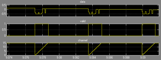
Simulink Sink library blocks display the results of the DDC simulation. The Scope block displays the raw output from the DDC design. The design has TDM outputs and all the data shows as data, valid and channel signals.
At each clock cycle, the value on the data wire either carries a genuine data output, or data that you can safely discard. The valid signal differentiates between these two cases. If the data is valid, the channel wire identifies the channel where the data belongs. Thus, you can use the valid and channel wires to filter the data. The ChanView block automates this task and decodes 16 channels of data to output channels 0 and 15. The block decimates these channels by the same rate as the whole filter line up and passes to a spectrum scope block (OutSpectrum) that examines the behavior in the frequency domain.
DDC DecimatingCIC and Scale Blocks
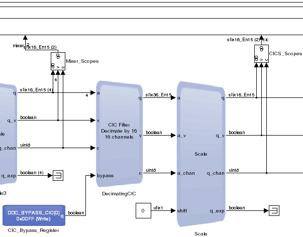
Two main blocks exist—the DecimatingCIC and the Scale block. To configure the CIC Filter, double click on the DecimatingCIC block.
The input sample rate is still the same as the data from the antenna. The dspb_ddc.SampleRate variable specifies the input sample rate. The number of channels, dspb_ddc.ChanCount, is a variable set to 16. The CIC filter has 5 stages, and performs decimation by a factor of 16. 1/16 in the dialog box indicates that the output rate is 1/16th of the input sample rate. The CIC parameter differential delay controls how many delays each CIC section uses—nearly always set to 1.
The CIC has no registers to configure, therefore no memory map elements exist.
The input data is a vector of four elements, so DSP Builder builds the decimating CIC from four separate CICs, each operating on four channels. The decimation behavior reduces the data rate at the output, therefore all 16 data samples (now at 61.44/16 MSPS each channel) can fit onto 1 wire.
The DecimatingCIC block multiplexes the results from each of the internal CIC filters onto a single wire. That is, four channels from vector element 1, followed by the four channels from vector element 2. DSP Builder packs the data onto a single TDM wire. Data is active for 25% of the cycles because the aggregate sample rate is now 61.44 MSPS × 16 channels/16 decimation = 61.44 MSPS and the clock rate for the system is 245.76 MHz.
Bursts of data occur, with 16 contiguous samples followed by a gap. Each burst is tagged with the valid signal. Also the channel indicator shows that the channel order is 0..15.
The number of input integrator sections is 4, and the number of output comb sections is 1. The lower data rate reduces the size of the overall group of 4 CICs. The Help page also reports the gain for the DCIC to be 1,048,576 or approximately 2^20. The Help page also shows how DSP Builder combines the four channels of input data on a single output data channel. The comb section utilization (from the DSP Builder menu) confirms the 25% calculation for the folding factor.
The Scale block reduces the output width in bits of the CIC results.
In this case, the design requires no variable shifting operation, so it uses a Simulink constant to tie the shift input to 0. However, because the gain through the DecimatingCIC block is approximately 2^20 division of the output, enter a scalar value -20 for the Number of bits to shift left in the dialog box to perform data.
DDC Decimating FIR Blocks
The last part of the DDC datapath comprises two decimating finite impulse response (FIR) blocks (DecimatingFIR1 and DecimatingFIR2) and their corresponding scale blocks (Scale1 and Scale2).
These two stages are very similar, the first filter typically compensates for the undesirable pass band response of the CIC filter, and the second FIR fine tunes the response that the waveform specification requires.
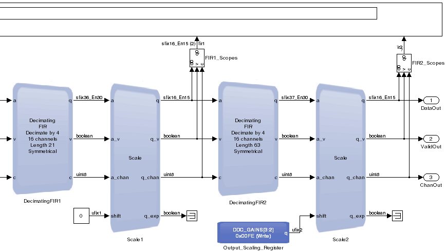
The first decimating FIR decimates by a factor of 4.
The input rate per channel is the output sample rate of the decimating CIC, which is 16 times lower than the raw sample rate from the antenna.
This filter performs decimation by a factor of 4 and the calculations reduce the size of the FIR filter. 16 channels exist to process and the coefficients are symmetrical.
The Coefficients field contains information that passes as a MATLAB fixed-point object (fi), which contains the data, and also the size and precision of each coefficient. Specifying an array of floating-point objects in the square brackets to the constructor to achieve this operation. The length of this array is the number of taps in the filter. At the end of this expression, the numbers 1, 16, 15 indicate that the fixed-point object is signed, and has 16-bit wide elements of which 15 are fractional bits.
For more information about fi objects, refer to the MATLAB Help.
This simple design uses a low-pass filter. In a real design, more careful generation of coefficients may be necessary.
The output of the FIR filter fits onto a single wire, but because the data reduces further, there is a longer gap between frames of data.
Access a report on the generated FIR filter from the Help page.
You can scroll down in the Help page to view the port interface details. These match the hardware block, although the RTL has additional ports for clock, reset, and the bus interface.
The report shows that the input data format uses a single channel repeating every 64 clock cycles and the output data is on a single channel repeating every 256 clock cycles.
Details of the memory map include the addresses DSP Builder requires to set up the filter parameters with an external microprocessor.
You can show the total estimated resources by clicking on the DSP Builder menu, pointing to Resources, and clicking Device. Intel estimates this filter to use 338 LUT4s, 1 18×18 multiplier and 7844 bits of RAM.
The Scale1 block that follows the DecimatingFIR1 block performs a similar function to the DecimatingCIC block.
The DecimatingFIR2 block performs a second level of decimation, in a very similar way to DecimatingFIR1. The coefficients use a MATLAB function. This function (fir1) returns an array of 63 doubles representing a low pass filter with cut off at 0.22. You can wrap this result in a fi object:
fi(fir1(62, 0.22),1,16,15)