External Memory Interfaces (EMIF) IP User Guide: Agilex™ 5 FPGAs and SoCs
A newer version of this document is available. Customers should click here to go to the newest version.
3.2.4. Agilex™ 5 EMIF Architecture: I/O Lane
| Pin Index | Lane | Sub-bank Location |
|---|---|---|
| 0-11 | 0 | Bottom |
| 12-23 | 1 | |
| 24-35 | 2 | |
| 36-47 | 3 | |
| 48-59 | 4 | Top |
| 60-71 | 5 | |
| 72-83 | 6 | |
| 84-95 | 7 |
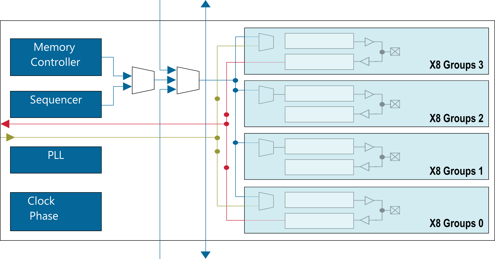
Each I/O lane can implement one x8/x9 read capture group (DQS group), with two pins functioning as the read capture clock/strobe pair (DQS T/DQS C), and up to 10 pins functioning as data pins (DQ and DM pins). To implement a x18 group, you can use multiple lanes within the same sub-bank.
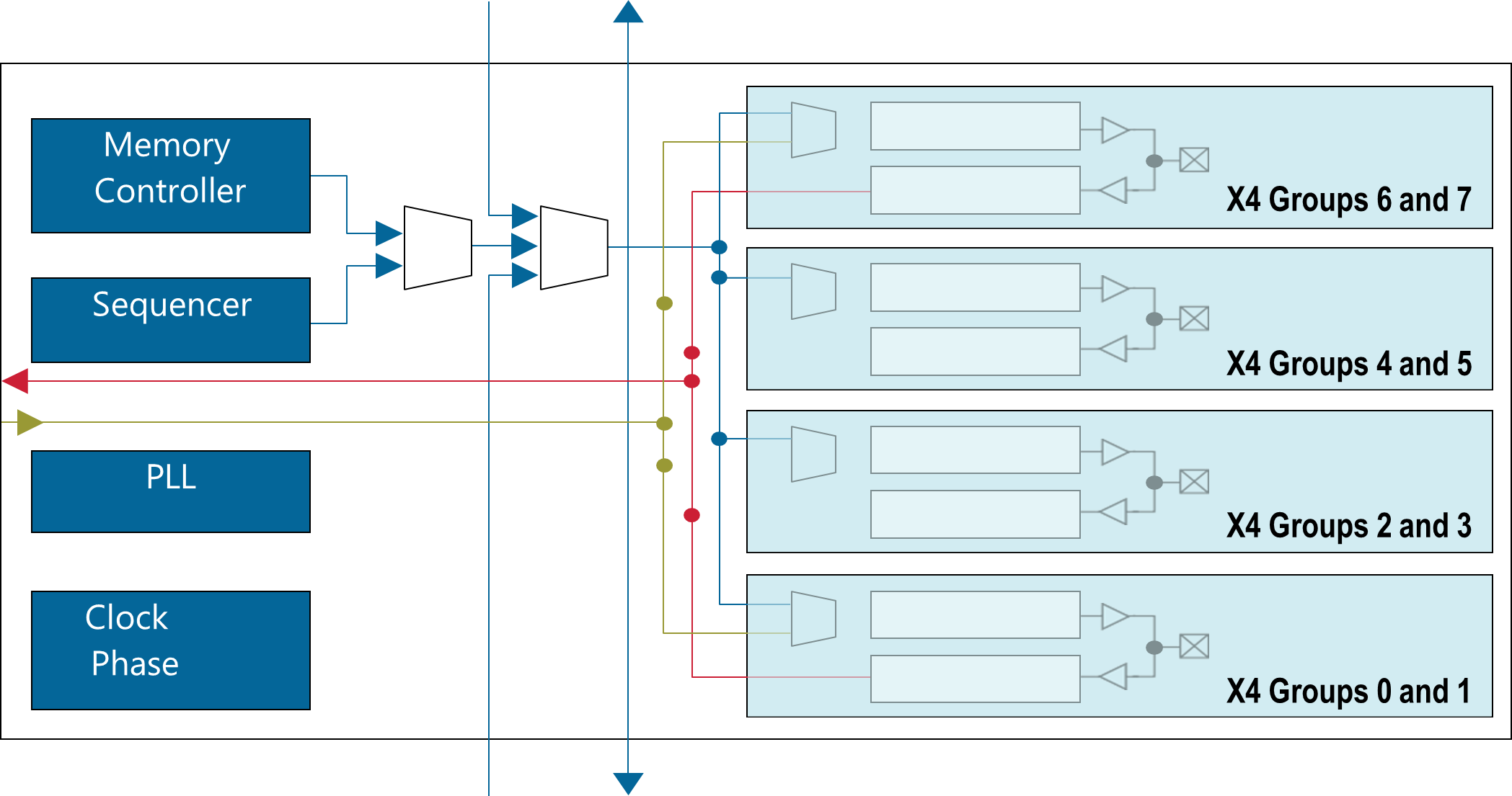
It is also possible to implement a pair of x4 groups in a lane. In this case, four pins function as clock/strobe pair, and 8 pins function as data pins. DM is not available for x4 groups. There must be an even number of x4 groups for each interface.
For x4 groups, you must place DQS0 and DQS1 in the same I/O lane as a pair. Similarly, DQS2 and DQS3 must be paired. In general, DQS(x) and DQS(x+1) must be paired in the same I/O lane.
For DQ and DQS pin assignments for various configurations, refer to the Agilex™ 5 device pin tables.
| Group Size | Number of Lanes Used | Maximum Number of Data Pins per Group |
|---|---|---|
| x8 / x9 | 1 | 10 |
| x18 | 2 | 22 |
| pair of x4 | 1 | 4 per group, 8 per lane |

