2.2.1. Building Hardware Design in Platform Designer Overview
2.2.2. Building Hardware Design in Platform Designer — Manual Instantiation
2.2.3. Building Hardware Design in Platform Designer — Board-Aware Flow
2.2.4. Building Hardware Design in Platform Designer — Configurable Example Design
2.2.5. Building Software Design with Ashling* RiscFree* IDE for Altera® FPGAs
2.2.2.2.1. Adding Nios® V/m Processor IP
2.2.2.2.2. Adding On-Chip Memory II (RAM or ROM) IP
2.2.2.2.3. Adding JTAG UART IP
2.2.2.2.4. Adding Reset Release IP
2.2.2.2.5. Connect Interfaces and Signals
2.2.2.2.6. Clear System Warnings and Errors
2.2.2.2.7. Configuring the Reset Vector of the Nios® V Processor
2.2.2.2.8. Saving and Generating System HDL
2.2.3.2.1. Adding Nios® V/m Processor IP
2.2.3.2.2. Adding On-Chip Memory (RAM or ROM) IP
2.2.3.2.3. Adding JTAG UART IP
2.2.3.2.4. Adding System ID Peripheral IP
2.2.3.2.5. Adding Reset Release IP
2.2.3.2.6. Connect Interfaces and Signals
2.2.3.2.7. Clear System Warnings and Errors
2.2.3.2.8. Saving and Generating System HDL
3.2.1.1. Creating a New Project
3.2.1.2. Creating a Platform Designer System
Adding Nios® V/m Processor IP
Adding On-Chip Memory (RAM or ROM) IP
Adding JTAG UART IP
Adding System ID Peripheral IP
Connect Interfaces and Signals
Clear System Warnings and Errors
Configuring the Reset Vector of the Nios® V Processor
Saving and Generating System HDL
3.2.1.3. Configuring Assignment and Constraint
3.2.1.4. Compiling the Quartus® Prime Software Project
3.2.1.2. Creating a Platform Designer System
- Click New, select Qsys System File and click OK.
Figure 106. New WindowFigure 107. Default Platform Designer System
- In Clock Source IP, configure the Clock frequency as 50000000 Hz (50 MHz).
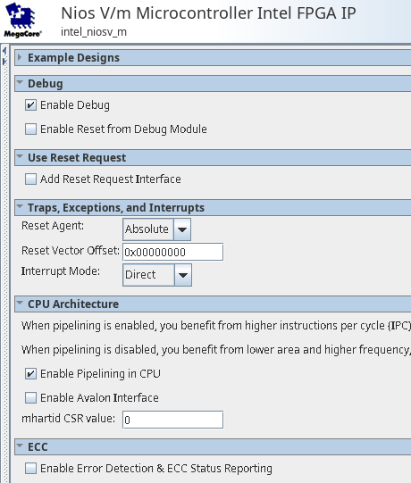
Adding Nios® V/m Processor IP
- Search for Nios V/m Processor in the IP Catalog.
- Add the Nios V/m Microcontroller IP under Processors and Peripherals > Embedded Processors section. The New IP Variation window appears.
- Click Finish to instantiate the processor. Leave it at the default settings.
Figure 108. Nios® V/m Processor IP Parameter Editor
Adding On-Chip Memory (RAM or ROM) IP
- Search for On-Chip Memory in the IP Catalog.
- Add the On-Chip Memory (RAM or ROM) IP under Basic Functions > On Chip Memory. The New IP Variation window appears.
- Configure the Total memory size as 159744.
- Turn on the option Enable non-default initialization file and provide the filename helloworld.hex.
- Leave other settings at default.
- Click Finish to instantiate the peripheral.
Figure 109. On-Chip Memory (RAM or ROM) IP Parameter Editor
Adding JTAG UART IP
- Search for JTAG UART in the IP Catalog.
- Add the JTAG UART IP under Interface Protocols > Serial section. The New IP Variation window appears.
- Click Finish to instantiate the peripheral. Leave it at the default settings.
Figure 110. JTAG UART Parameter Editor
Adding System ID Peripheral IP
- Search for System ID in the IP Catalog.
- Add the System ID Peripheral IP under Basic Function > Simulation; Debug and Verification > Debug and Performance section. The New IP Variation window appears.
- Click Finish to instantiate the peripheral. Leave it at the default settings.
Figure 111. System ID Parameter Editor
Connect Interfaces and Signals
Connect the clock source and Nios® V processor to the peripherals.
| IP | Host | Peripheral |
|---|---|---|
| Clock Source IP | clk | intel_niosv_m_0.clk |
| onchip_memory2_0.clk | ||
| jtag_uart_0.clk | ||
| sysid_qsys_0.clk | ||
| clk_reset | intel_niosv_m_0.reset | |
| onchip_memory2_0.reset1 | ||
| jtag_uart_0.reset | ||
| sysid_qsys_0.reset | ||
| Nios V/m Processor IP | platform_irq_x | jtag_uart_0.irq |
| instruction_manager | onchip_memory2_0.s1 | |
| data_manager | onchip_memory2_0.s1 | |
| jtag_uart_0.avalon_jtag_slave | ||
| sysid_qsys_0.control_slave |
Figure 112. Full System Connection
Clear System Warnings and Errors
- Navigate to the System menu bar.
- Click Assign Base Addresses.
Figure 113. Example of System Connectivity Issue
Configuring the Reset Vector of the Nios® V Processor
- Double click on Nios V Processor IP to open the IP Parameter Editor.
- Navigate to the Vectors tab.
- Configure as follows:
- Reset Agent: onchip_memory1_0.s1
- Reset Offset: 0x0
Figure 114. Reset Vector
Saving and Generating System HDL
- Navigate to the File menu bar.
- Click Save.
- Save your QSYS design as niosv_top.qsys and click Save.
- Click Generate HDL at the bottom right corner of the Platform Designer.
- Ensure that the Nios V processor hardware system is successfully generated.
Figure 115. Successful Generation
- The Platform Designer generates a folder named niosv_top, which stores the system generation files.
- Exit the Platform Designer and return to the project front page.
Figure 116. Generated Project Files