AN 847: Signal Tap Tutorial with Design Block Reuse: for Intel® Arria® 10 FPGA Development Board
ID
683712
Date
12/21/2020
Public
1. Introduction
2. Core Partition Reuse Debug—Developer
3. Core Partition Reuse Debug—Consumer
4. Root Partition Reuse Debug—Developer
5. Root Partition Reuse Debug—Consumer
6. AN 847: Signal Tap Tutorial with Design Block Reuse for Intel® Arria® 10 FPGA Development Board Archives
7. Document Revision History for AN 847: Signal Tap Tutorial with Design Block Reuse for Intel® Arria® 10 FPGA Development Board
2.1. Step 1: Creating a Core Partition
2.2. Step 2: Creating Partition Boundary Ports
2.3. Step 3: Compiling and Checking Debug Nodes
2.4. Step 4: Exporting the Core Partition and Creating the Black Box File
2.5. Step 5: Copying Files to Consumer Project
2.6. Step 6: Creating a Signal Tap File (Optional)
2.7. Step 7: Programming the Device and Verifying the Hardware
2.8. Step 8: Verifying Hardware with Signal Tap
3.1. Step 1: Adding Files and Running Synthesis
3.2. Step 2: Creating a Signal Tap File
3.3. Step 3: Creating a Partition for blinking_led_top
3.4. Step 4: Compiling the Design and Verifying Debug Nodes
3.5. Step 5: Programming the Device and Verifying the Hardware
3.6. Step 6: Verifying Hardware with Signal Tap
4.1. Step 1: Creating a Reserved Core Partition and Defining a Logic Lock Region
4.2. Step 2: Generating and Instantiating SLD JTAG Bridge Agent in the Root Partition
4.3. Step 3: Generating and Instantiating the SLD JTAG Bridge Host
4.4. Step 4: Generating HDL Instance of Signal Tap
4.5. Step 5: Compiling Export Root Partition and Copying Files to Consumer Project
4.6. Step 6: Programming the Device and Verifying the Hardware
4.7. Step 7: Generating a Signal Tap File for the Root Partition
4.8. Step 8: Verifying the Hardware with Signal Tap
5.1. Step 1: Adding Files to Customer Project
5.2. Step 2: Generating and Instantiating SLD JTAG Bridge Host in Reserved Core Partition
5.3. Step 3: Synthesizing, Creating Signal Tap File, and Compiling
5.4. Step 4: Programming the Device and Verifying the Hardware
5.5. Step 5: Verifying the Hardware of Reserved Core Partition with Signal Tap
5.6. Step 6: Verifying Hardware of Root Partition with Signal Tap
2.8. Step 8: Verifying Hardware with Signal Tap
- In the Signal Tap window, click File > Open, and open stp_core_partition_reuse.stp.
- Ensure that the development kit is powered ON and connected to the machine from which you open the Signal Tap logic analyzer.
- In the JTAG Chain Configuration tab, set up the JTAG connection to the board by clicking Setup and then selecting the USB-BlasterII under Hardware.
The device populates automatically.
Figure 23. JTAG Scan Configuration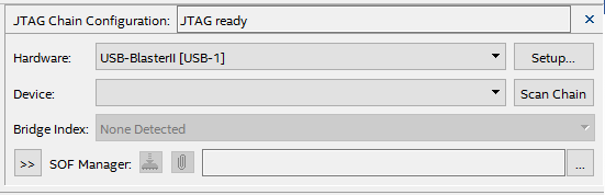 The Instance Manager window shows Ready to acquire.Figure 24. Instance Manager
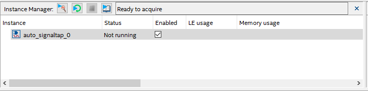
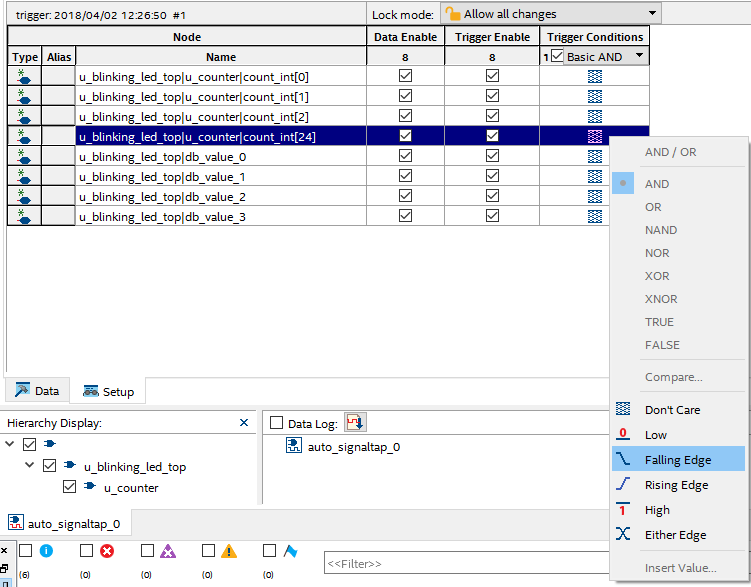
- To set the trigger condition, select count_int[24], right-click the column under Trigger Conditions, and set to Falling Edge.
Figure 25. Trigger Conditions
- Run analysis by clicking Processing > Run Analysis.
When the analysis finishes, the Waveform tab shows the captured data.
Figure 26. Waveform after Signal Tap Analysis
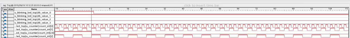
- The count_int[27:24] register in u_blinking_led_top|u_counter|count_int[27:24] drives u_blinking_led_top|u_blinking_led|value[3:0].
- The partition boundary ports created for each bit of value[3:0] are db_value_3, db_value_2, db_value_1, and db_value_0.
- The value of db_value_0 changes a cycle later after count_int[24] transitions to 0. The count_int[2:0] shows the transitioning of the counter during this process