AN 847: Signal Tap Tutorial with Design Block Reuse: for Intel® Arria® 10 FPGA Development Board
                    
                        ID
                        683712


                    Date
                    12/21/2020
                
                
                    Public


                        1. Introduction


                        2. Core Partition Reuse Debug—Developer


                        3. Core Partition Reuse Debug—Consumer


                        4. Root Partition Reuse Debug—Developer


                        5. Root Partition Reuse Debug—Consumer


                        6. AN 847: Signal Tap Tutorial with Design Block Reuse for Intel® Arria® 10 FPGA Development Board Archives


                        7. Document Revision History for AN 847: Signal Tap Tutorial with Design Block Reuse for Intel® Arria® 10 FPGA Development Board


                                2.1. Step 1: Creating a Core Partition


                                2.2. Step 2: Creating Partition Boundary Ports


                                2.3. Step 3: Compiling and Checking Debug Nodes


                                2.4. Step 4: Exporting the Core Partition and Creating the Black Box File


                                2.5. Step 5: Copying Files to Consumer Project


                                2.6. Step 6: Creating a Signal Tap File (Optional)


                                2.7. Step 7: Programming the Device and Verifying the Hardware


                                2.8. Step 8: Verifying Hardware with Signal Tap


                                3.1. Step 1: Adding Files and Running Synthesis


                                3.2. Step 2: Creating a Signal Tap File


                                3.3. Step 3: Creating a Partition for blinking_led_top


                                3.4. Step 4: Compiling the Design and Verifying Debug Nodes


                                3.5. Step 5: Programming the Device and Verifying the Hardware


                                3.6. Step 6: Verifying Hardware with Signal Tap


                                4.1. Step 1: Creating a Reserved Core Partition and Defining a Logic Lock Region


                                4.2. Step 2: Generating and Instantiating SLD JTAG Bridge Agent in the Root Partition


                                4.3. Step 3: Generating and Instantiating the SLD JTAG Bridge Host


                                4.4. Step 4: Generating HDL Instance of Signal Tap


                                4.5. Step 5: Compiling Export Root Partition and Copying Files to Consumer Project


                                4.6. Step 6: Programming the Device and Verifying the Hardware


                                4.7. Step 7: Generating a Signal Tap File for the Root Partition


                                4.8. Step 8: Verifying the Hardware with Signal Tap


                                5.1. Step 1: Adding Files to Customer Project


                                5.2. Step 2: Generating and Instantiating SLD JTAG Bridge Host in Reserved Core Partition


                                5.3. Step 3: Synthesizing, Creating Signal Tap File, and Compiling


                                5.4. Step 4: Programming the Device and Verifying the Hardware


                                5.5. Step 5: Verifying the Hardware of Reserved Core Partition with Signal Tap


                                5.6. Step 6: Verifying Hardware of Root Partition with Signal Tap


                2.4. Step 4: Exporting the Core Partition and Creating the Black Box File
 After compilation, you export the core partition and create a supporting black box port definitions file.  This tutorial reuses the final compilation snapshot. 
  
 
  -  Click Project > Export Design Partition. Select blinking_led_top for the Partition name, and the final Snapshot for export. 
    
 
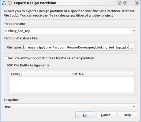
       - Confirm blinking_led_top.qdb as the Partition Database File name, and then click OK. The final blinking_led.qdb that you export preserves the placement and routing information from the Developer project reused in the Consumer project.
 -  To create the black box file, click File > New, select SystemVerilog HDL File under Design Files, and then click OK. 
    A blank .sv file opens to allow you to enter the port definitions for the partition you export and the partition boundary ports created in Step 3: Compiling and Checking Debug Nodes.
 -  Include any Verilog parameters or VHDL generics in the definition. The port definitions in the black box file must look just like the original, without the logic RTL. 
    
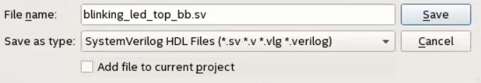
module blinking_led_top( output [3:0] value, input clock, output db_count_0, output db_count_1, output db_count_2, output db_count_24, output db_value_0, output db_value_1, output db_value_2, output db_value_3 ); endmodule -  Save the black box file as blinking_led_top_bb.sv. When saving this file, turn off the option to Add file to current project.