AN 847: Signal Tap Tutorial with Design Block Reuse: for Intel® Arria® 10 FPGA Development Board
ID
683712
Date
12/21/2020
Public
1. Introduction
2. Core Partition Reuse Debug—Developer
3. Core Partition Reuse Debug—Consumer
4. Root Partition Reuse Debug—Developer
5. Root Partition Reuse Debug—Consumer
6. AN 847: Signal Tap Tutorial with Design Block Reuse for Intel® Arria® 10 FPGA Development Board Archives
7. Document Revision History for AN 847: Signal Tap Tutorial with Design Block Reuse for Intel® Arria® 10 FPGA Development Board
2.1. Step 1: Creating a Core Partition
2.2. Step 2: Creating Partition Boundary Ports
2.3. Step 3: Compiling and Checking Debug Nodes
2.4. Step 4: Exporting the Core Partition and Creating the Black Box File
2.5. Step 5: Copying Files to Consumer Project
2.6. Step 6: Creating a Signal Tap File (Optional)
2.7. Step 7: Programming the Device and Verifying the Hardware
2.8. Step 8: Verifying Hardware with Signal Tap
3.1. Step 1: Adding Files and Running Synthesis
3.2. Step 2: Creating a Signal Tap File
3.3. Step 3: Creating a Partition for blinking_led_top
3.4. Step 4: Compiling the Design and Verifying Debug Nodes
3.5. Step 5: Programming the Device and Verifying the Hardware
3.6. Step 6: Verifying Hardware with Signal Tap
4.1. Step 1: Creating a Reserved Core Partition and Defining a Logic Lock Region
4.2. Step 2: Generating and Instantiating SLD JTAG Bridge Agent in the Root Partition
4.3. Step 3: Generating and Instantiating the SLD JTAG Bridge Host
4.4. Step 4: Generating HDL Instance of Signal Tap
4.5. Step 5: Compiling Export Root Partition and Copying Files to Consumer Project
4.6. Step 6: Programming the Device and Verifying the Hardware
4.7. Step 7: Generating a Signal Tap File for the Root Partition
4.8. Step 8: Verifying the Hardware with Signal Tap
5.1. Step 1: Adding Files to Customer Project
5.2. Step 2: Generating and Instantiating SLD JTAG Bridge Host in Reserved Core Partition
5.3. Step 3: Synthesizing, Creating Signal Tap File, and Compiling
5.4. Step 4: Programming the Device and Verifying the Hardware
5.5. Step 5: Verifying the Hardware of Reserved Core Partition with Signal Tap
5.6. Step 6: Verifying Hardware of Root Partition with Signal Tap
2.6. Step 6: Creating a Signal Tap File (Optional)
In this step, you configure the Signal Tap logic analyzer, and then tap partition boundary ports and pre-synthesis nodes from the parent partition to debug in the Developer project. Configuring the Signal Tap logic analyzer includes adding a reference clock and specifying acquisition settings.
- In the Intel® Quartus® Prime Pro Edition software, click Tools > Signal Tap Logic Analyzer.
Figure 15. Signal Tap Logic Analyzer Window
- In the Instance Manager, click auto_signaltap_0.
- In the Setup tab, double-click to launch the Node Finder.
- In the Node Finder, type * in the Named field, set Filter to Signal Tap: pre-synthesis, and then click Search.
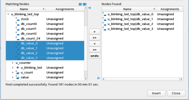
- In the Matching Nodes list, expand u_blinking_led_top. Select db_value_0, db_value_1, db_value_2, and db_value_3.
Figure 16. Node Finder Copy Nodes
- In the Matching Nodes list, expand the u_blinking_led_top > u_counter > count_int.
- From the node list, select count_int[0], count_int[1], count_int[2], and count_int[24], and insert the nodes by clicking >.
- Click Insert, and then Close.
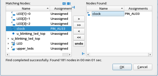
- In the Signal Tap window, under Signal Configuration, click (…) next to the Clock field.
- In the Node Finder, search for *, and select the clock.
- Click >, and then click OK to close.
Figure 17. Clock Signal in Node Finder
- Leave all other options as default under Signal Configuration.
- Go to File > Save and save the file as stp_core_partition_reuse.stp.
A dialog box appears asking if you want to enable Signal Tap file for the project.
- Click Yes, and close the file.
- Click Compile Design on the Compilation Dashboard.