AN 847: Signal Tap Tutorial with Design Block Reuse: for Intel® Arria® 10 FPGA Development Board
ID
683712
Date
12/21/2020
Public
1. Introduction
2. Core Partition Reuse Debug—Developer
3. Core Partition Reuse Debug—Consumer
4. Root Partition Reuse Debug—Developer
5. Root Partition Reuse Debug—Consumer
6. AN 847: Signal Tap Tutorial with Design Block Reuse for Intel® Arria® 10 FPGA Development Board Archives
7. Document Revision History for AN 847: Signal Tap Tutorial with Design Block Reuse for Intel® Arria® 10 FPGA Development Board
2.1. Step 1: Creating a Core Partition
2.2. Step 2: Creating Partition Boundary Ports
2.3. Step 3: Compiling and Checking Debug Nodes
2.4. Step 4: Exporting the Core Partition and Creating the Black Box File
2.5. Step 5: Copying Files to Consumer Project
2.6. Step 6: Creating a Signal Tap File (Optional)
2.7. Step 7: Programming the Device and Verifying the Hardware
2.8. Step 8: Verifying Hardware with Signal Tap
3.1. Step 1: Adding Files and Running Synthesis
3.2. Step 2: Creating a Signal Tap File
3.3. Step 3: Creating a Partition for blinking_led_top
3.4. Step 4: Compiling the Design and Verifying Debug Nodes
3.5. Step 5: Programming the Device and Verifying the Hardware
3.6. Step 6: Verifying Hardware with Signal Tap
4.1. Step 1: Creating a Reserved Core Partition and Defining a Logic Lock Region
4.2. Step 2: Generating and Instantiating SLD JTAG Bridge Agent in the Root Partition
4.3. Step 3: Generating and Instantiating the SLD JTAG Bridge Host
4.4. Step 4: Generating HDL Instance of Signal Tap
4.5. Step 5: Compiling Export Root Partition and Copying Files to Consumer Project
4.6. Step 6: Programming the Device and Verifying the Hardware
4.7. Step 7: Generating a Signal Tap File for the Root Partition
4.8. Step 8: Verifying the Hardware with Signal Tap
5.1. Step 1: Adding Files to Customer Project
5.2. Step 2: Generating and Instantiating SLD JTAG Bridge Host in Reserved Core Partition
5.3. Step 3: Synthesizing, Creating Signal Tap File, and Compiling
5.4. Step 4: Programming the Device and Verifying the Hardware
5.5. Step 5: Verifying the Hardware of Reserved Core Partition with Signal Tap
5.6. Step 6: Verifying Hardware of Root Partition with Signal Tap
4.1. Step 1: Creating a Reserved Core Partition and Defining a Logic Lock Region
- In the Intel® Quartus® Prime Pro Edition software, click File > Open Project, and open the a10_pcie_devkit_design_block_reuse_stp/Root_Partition_Reuse/Developer/top.qpf project file.
- On the Compilation Dashboard, click Analysis & Synthesis to synthesize the design. When synthesis is complete, the Compilation Dashboard displays a check mark.
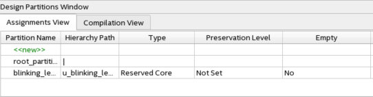
- In the Project Navigator, right-click the u_blinking_led_top instance in the Hierarchy tab, and then click Design Partition > Reserved Core. A design partition icon appears next to each instance you assign.
Note: If the Design Partition Window is not visible on the GUI, click Assignments > Design Partitions Window.Figure 34. Set Reserved Core Partition Type
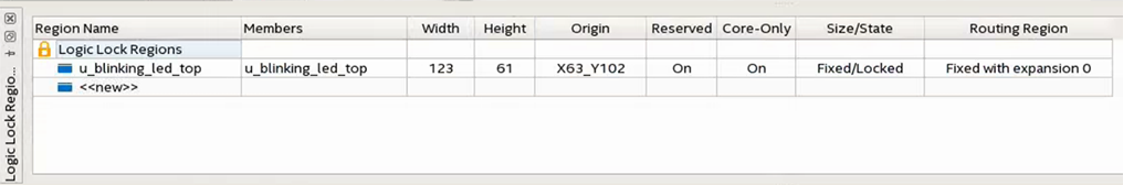
- Right-click the u_blinking_led_top instance in the Project Navigator, and click Logic Lock Region > Create New Logic Lock Region.
- To modify the region properties, click Assignments > Logic Lock Regions Window.
- Change the Width to 123, and the Height to 61.
- In the Origin column, specify X63_Y102.
- Enable the Reserved and Core-Only options.
- In the Size/State column, specify Fixed/Locked.
- Click the Routing Region cell. The Logic Lock Routing Region Settings dialog box appears.
- Specify Fixed with expansion with Expansion Length of 0 for the Routing Type. The actual size and location are arbitrary for this tutorial. However, you can view and adjust the Logic Lock Region shape in the Chip Planner.
Figure 35. Logic Lock Regions Window