AN 847: Signal Tap Tutorial with Design Block Reuse: for Intel® Arria® 10 FPGA Development Board
                    
                        ID
                        683712


                    Date
                    12/21/2020
                
                
                    Public


                        1. Introduction


                        2. Core Partition Reuse Debug—Developer


                        3. Core Partition Reuse Debug—Consumer


                        4. Root Partition Reuse Debug—Developer


                        5. Root Partition Reuse Debug—Consumer


                        6. AN 847: Signal Tap Tutorial with Design Block Reuse for Intel® Arria® 10 FPGA Development Board Archives


                        7. Document Revision History for AN 847: Signal Tap Tutorial with Design Block Reuse for Intel® Arria® 10 FPGA Development Board


                                2.1. Step 1: Creating a Core Partition


                                2.2. Step 2: Creating Partition Boundary Ports


                                2.3. Step 3: Compiling and Checking Debug Nodes


                                2.4. Step 4: Exporting the Core Partition and Creating the Black Box File


                                2.5. Step 5: Copying Files to Consumer Project


                                2.6. Step 6: Creating a Signal Tap File (Optional)


                                2.7. Step 7: Programming the Device and Verifying the Hardware


                                2.8. Step 8: Verifying Hardware with Signal Tap


                                3.1. Step 1: Adding Files and Running Synthesis


                                3.2. Step 2: Creating a Signal Tap File


                                3.3. Step 3: Creating a Partition for blinking_led_top


                                3.4. Step 4: Compiling the Design and Verifying Debug Nodes


                                3.5. Step 5: Programming the Device and Verifying the Hardware


                                3.6. Step 6: Verifying Hardware with Signal Tap


                                4.1. Step 1: Creating a Reserved Core Partition and Defining a Logic Lock Region


                                4.2. Step 2: Generating and Instantiating SLD JTAG Bridge Agent in the Root Partition


                                4.3. Step 3: Generating and Instantiating the SLD JTAG Bridge Host


                                4.4. Step 4: Generating HDL Instance of Signal Tap


                                4.5. Step 5: Compiling Export Root Partition and Copying Files to Consumer Project


                                4.6. Step 6: Programming the Device and Verifying the Hardware


                                4.7. Step 7: Generating a Signal Tap File for the Root Partition


                                4.8. Step 8: Verifying the Hardware with Signal Tap


                                5.1. Step 1: Adding Files to Customer Project


                                5.2. Step 2: Generating and Instantiating SLD JTAG Bridge Host in Reserved Core Partition


                                5.3. Step 3: Synthesizing, Creating Signal Tap File, and Compiling


                                5.4. Step 4: Programming the Device and Verifying the Hardware


                                5.5. Step 5: Verifying the Hardware of Reserved Core Partition with Signal Tap


                                5.6. Step 6: Verifying Hardware of Root Partition with Signal Tap


                2.2. Step 2: Creating Partition Boundary Ports
 Follow these steps to create partition boundary ports to expose signals from the parent partition. 
  
 
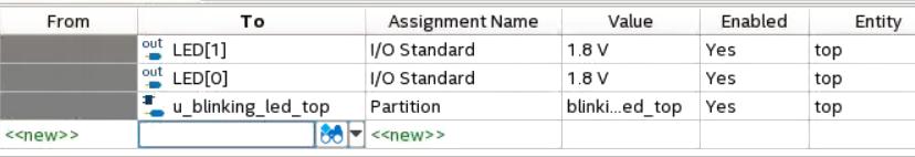
  - In the Intel® Quartus® Prime software, click Assignments > Assignment Editor.
 - In the Assignment Editor, locate the <<new>> row at the bottom of the list.
 -  Double-click the To column, and then click the Node Finder button. 
    Figure 9. Assignment Editor
 
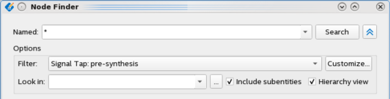
       -  In the Node Finder, type * in the Named field, set Filter to  Signal Tap: pre-synthesis, and then click Search. 
    Figure 10. Node Finder Search
 
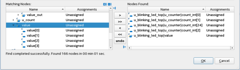
      The Matching Nodes list shows signals that match the search criteria. - In the Matching Nodes list, expand u_blinking_led_top > u_counter > count_int.
 - Select count_int[0], count_int[1], count_int[2], and count_int[24], and click > to move them to the Nodes Found list. Do not click OK.
 -  In the Matching Nodes list, expand u_blinking_led_top, and select value. Click >.  
    Figure 11. Node Finder Copy Nodes
 
       - Click OK to close the Node Finder.
 -  In the Assignment Editor window, for each of these nodes, populate information for rest of the columns. 
    For example, for node u_blinking_led_top|u_blinking_led|value, double-click Assignment Name and select Create Partition Boundary Ports. Double-click value to provide a port name db_value. Leave rest of the columns as default.Figure 12. Assignment Editor
 
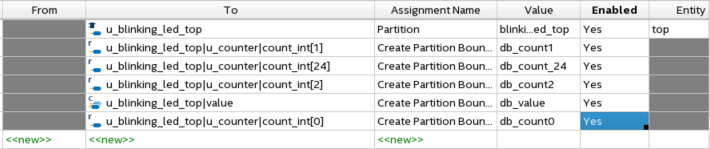
       - Click File > Save to save all changes.
 -  Optionally, you can verify the following assignments in /Core_Partition_Reuse/Developer/top.qsf.  
    
set_instance_assignment -name CREATE_PARTITION_BOUNDARY_PORTS db_count_1 \ -to u_blinking_led_top|u_counter|count_int[1] set_instance_assignment -name CREATE_PARTITION_BOUNDARY_PORTS db_count_24 \ -to u_blinking_led_top|u_counter|count_int[24] set_instance_assignment -name CREATE_PARTITION_BOUNDARY_PORTS db_count_2 \ -to u_blinking_led_top|u_counter|count_int[2] set_instance_assignment -name CREATE_PARTITION_BOUNDARY_PORTS db_value \ -to u_blinking_led_top|value set_instance_assignment -name CREATE_PARTITION_BOUNDARY_PORTS db_count_0 \ -to u_blinking_led_top|u_counter|count_int[0]