AN 847: Signal Tap Tutorial with Design Block Reuse: for Intel® Arria® 10 FPGA Development Board
ID
683712
Date
12/21/2020
Public
1. Introduction
2. Core Partition Reuse Debug—Developer
3. Core Partition Reuse Debug—Consumer
4. Root Partition Reuse Debug—Developer
5. Root Partition Reuse Debug—Consumer
6. AN 847: Signal Tap Tutorial with Design Block Reuse for Intel® Arria® 10 FPGA Development Board Archives
7. Document Revision History for AN 847: Signal Tap Tutorial with Design Block Reuse for Intel® Arria® 10 FPGA Development Board
2.1. Step 1: Creating a Core Partition
2.2. Step 2: Creating Partition Boundary Ports
2.3. Step 3: Compiling and Checking Debug Nodes
2.4. Step 4: Exporting the Core Partition and Creating the Black Box File
2.5. Step 5: Copying Files to Consumer Project
2.6. Step 6: Creating a Signal Tap File (Optional)
2.7. Step 7: Programming the Device and Verifying the Hardware
2.8. Step 8: Verifying Hardware with Signal Tap
3.1. Step 1: Adding Files and Running Synthesis
3.2. Step 2: Creating a Signal Tap File
3.3. Step 3: Creating a Partition for blinking_led_top
3.4. Step 4: Compiling the Design and Verifying Debug Nodes
3.5. Step 5: Programming the Device and Verifying the Hardware
3.6. Step 6: Verifying Hardware with Signal Tap
4.1. Step 1: Creating a Reserved Core Partition and Defining a Logic Lock Region
4.2. Step 2: Generating and Instantiating SLD JTAG Bridge Agent in the Root Partition
4.3. Step 3: Generating and Instantiating the SLD JTAG Bridge Host
4.4. Step 4: Generating HDL Instance of Signal Tap
4.5. Step 5: Compiling Export Root Partition and Copying Files to Consumer Project
4.6. Step 6: Programming the Device and Verifying the Hardware
4.7. Step 7: Generating a Signal Tap File for the Root Partition
4.8. Step 8: Verifying the Hardware with Signal Tap
5.1. Step 1: Adding Files to Customer Project
5.2. Step 2: Generating and Instantiating SLD JTAG Bridge Host in Reserved Core Partition
5.3. Step 3: Synthesizing, Creating Signal Tap File, and Compiling
5.4. Step 4: Programming the Device and Verifying the Hardware
5.5. Step 5: Verifying the Hardware of Reserved Core Partition with Signal Tap
5.6. Step 6: Verifying Hardware of Root Partition with Signal Tap
2.3. Step 3: Compiling and Checking Debug Nodes
- Click Compile Design on the Compilation Dashboard.
Figure 13. Full Compilation in Compilation Dashboard
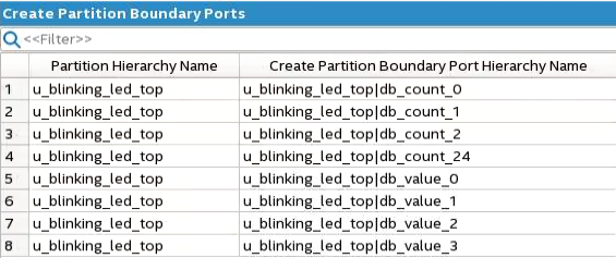
- Open the compilation report by clicking Processing > Compilation Report.
- Under Table of Contents, find Synthesis > In-System Debugging > Create Partition Boundary Ports.
Figure 14. Create Partition Boundary Ports