AN 847: Signal Tap Tutorial with Design Block Reuse: for Intel® Arria® 10 FPGA Development Board
                    
                        ID
                        683712


                    Date
                    12/21/2020
                
                
                    Public


                        1. Introduction


                        2. Core Partition Reuse Debug—Developer


                        3. Core Partition Reuse Debug—Consumer


                        4. Root Partition Reuse Debug—Developer


                        5. Root Partition Reuse Debug—Consumer


                        6. AN 847: Signal Tap Tutorial with Design Block Reuse for Intel® Arria® 10 FPGA Development Board Archives


                        7. Document Revision History for AN 847: Signal Tap Tutorial with Design Block Reuse for Intel® Arria® 10 FPGA Development Board


                                2.1. Step 1: Creating a Core Partition


                                2.2. Step 2: Creating Partition Boundary Ports


                                2.3. Step 3: Compiling and Checking Debug Nodes


                                2.4. Step 4: Exporting the Core Partition and Creating the Black Box File


                                2.5. Step 5: Copying Files to Consumer Project


                                2.6. Step 6: Creating a Signal Tap File (Optional)


                                2.7. Step 7: Programming the Device and Verifying the Hardware


                                2.8. Step 8: Verifying Hardware with Signal Tap


                                3.1. Step 1: Adding Files and Running Synthesis


                                3.2. Step 2: Creating a Signal Tap File


                                3.3. Step 3: Creating a Partition for blinking_led_top


                                3.4. Step 4: Compiling the Design and Verifying Debug Nodes


                                3.5. Step 5: Programming the Device and Verifying the Hardware


                                3.6. Step 6: Verifying Hardware with Signal Tap


                                4.1. Step 1: Creating a Reserved Core Partition and Defining a Logic Lock Region


                                4.2. Step 2: Generating and Instantiating SLD JTAG Bridge Agent in the Root Partition


                                4.3. Step 3: Generating and Instantiating the SLD JTAG Bridge Host


                                4.4. Step 4: Generating HDL Instance of Signal Tap


                                4.5. Step 5: Compiling Export Root Partition and Copying Files to Consumer Project


                                4.6. Step 6: Programming the Device and Verifying the Hardware


                                4.7. Step 7: Generating a Signal Tap File for the Root Partition


                                4.8. Step 8: Verifying the Hardware with Signal Tap


                                5.1. Step 1: Adding Files to Customer Project


                                5.2. Step 2: Generating and Instantiating SLD JTAG Bridge Host in Reserved Core Partition


                                5.3. Step 3: Synthesizing, Creating Signal Tap File, and Compiling


                                5.4. Step 4: Programming the Device and Verifying the Hardware


                                5.5. Step 5: Verifying the Hardware of Reserved Core Partition with Signal Tap


                                5.6. Step 6: Verifying Hardware of Root Partition with Signal Tap


                5.6. Step 6: Verifying Hardware of Root Partition with Signal Tap
- Go to the shell from where you opened the Intel® Quartus® Prime software.
 -  In the shell, go to directory   a10_pcie_devkit_design_block_reuse_stp/Root_Partition_Reuse/Consumer  , and then run the following command: 
    
quartus_stp top --create_signaltap_hdl_file --stp_file \ stp_root_partition.stp - In the Signal Tap window, click File > Open, and open the stp_root_partition.stp file, which you created in the previous step.
 - Ensure that the development kit is powered ON and connected to the machine from which you open the Signal Tap logic analyzer.
 - Verify that Bridge Index is set to None in the JTAG Chain Configuration window
 - To set the trigger condition, select the count[0], count[1], count[2], and count[3] signals, right-click the column under Trigger Conditions, and select Falling Edge.
 -  Run analysis by clicking Processing > Run Analysis. 
    When the analysis finishes, the Waveform tab shows the captured data.
 -  Verify the transition of the nodes in the root partition. 
    Figure 45. Waveforms for Root Partition Nodes in Consumer Project
 
       
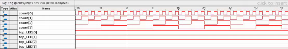
In this tutorial design, the count[3:0] signals represent the counter in the root partition, and the top_LED signals represent the green LEDs on the board, which also map to the top-level (root) design. After the trigger activates, only one of the top_LED bits is low, at any time.
If the implementation succeeds, the Consumer project behaves identically to the Developer project.