Arria® 10 GX Transceiver Signal Integrity Development Kit User Guide
ID
683553
Date
12/01/2025
Public
1. About This Development Kit
2. Getting Started
3. Development Board Setup
4. Board Update Portal
5. Board Components
6. Board Test System
7. Document Revision History for the Arria® 10 GX Transceiver Signal Integrity Development Kit User Guide
A. Programming the Flash Memory Device
B. Safety and Regulatory Compliance Information
A.1. CFI Flash Memory Map
A.2. Preparing Design Files for Flash Programming
A.3. Creating Flash Files Using the Nios® II EDS
A.4. Programming Flash Memory Using the Board Update Portal
A.5. Programming Flash Memory Using the Nios II EDS
A.6. Restoring the Flash Device to the Factory Settings
A.7. Restoring the MAX® V CPLD to the Factory Settings
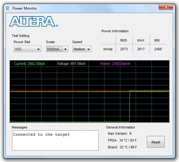
6.4.8. Power Monitoring
The Power Monitor measures and reports current power information and communicates with the MAX V device on the board through the JTAG bus. A power monitor circuit attached to the MAX V device allows you to measure the power that the FPGA is consuming.
To start the application, click the Power Monitor icon in the Board Test System application. You can also run the Power Monitor as a stand-alone application. The PowerMonitor.exe reside in the <package dir>\examples\board_test_system directory
Note: You cannot run the stand-alone power application and the BTS application at the same time. Also, you cannot run power and clock interface at the same time.
Figure 24. Power Monitor