Arria® 10 GX Transceiver Signal Integrity Development Kit User Guide
ID
683553
Date
12/01/2025
Public
1. About This Development Kit
2. Getting Started
3. Development Board Setup
4. Board Update Portal
5. Board Components
6. Board Test System
7. Document Revision History for the Arria® 10 GX Transceiver Signal Integrity Development Kit User Guide
A. Programming the Flash Memory Device
B. Safety and Regulatory Compliance Information
A.1. CFI Flash Memory Map
A.2. Preparing Design Files for Flash Programming
A.3. Creating Flash Files Using the Nios® II EDS
A.4. Programming Flash Memory Using the Board Update Portal
A.5. Programming Flash Memory Using the Nios II EDS
A.6. Restoring the Flash Device to the Factory Settings
A.7. Restoring the MAX® V CPLD to the Factory Settings
5.4.1. FPGA Programming over Embedded USB-Blaster
The figure below shows the high-level conceptual block diagram for the embedded USB-Blaster.
Figure 4. USB-Blaster Conceptual Block Diagram
The figure below shows a more detailed schematic block diagram for the embedded USB-Blaster interfacing to the Intel® Arria® 10 GX FPGA device.
Figure 5. Detailed USB-Blaster to FPGA Schematic
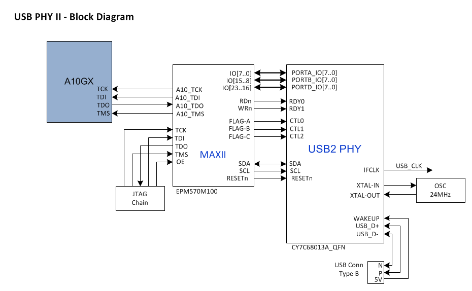
The embedded USB Blaster core for USB-based configuration of the Intel® Arria® 10 GX FPGA device is implemented using a TYPE B USB connector, a CY7C68013A USB2 PHY device, and an Altera MAX II EPM570M100 CPLD. This will allow configuration of the Intel® Arria® 10 GX FPGA device using a USB cable directly connected to a PC running Intel® Quartus® Prime software without requiring the external USB Blaster dongle. This design will convert USB data to interface with the Intel® Arria® 10 GX FPGA’s dedicated JTAG port. An LED (D4) is provided to indicate USB Blaster activity. The embedded USB blaster is automatically disabled when an external USB Blaster dongle is connected to the JTAG chain.