Arria® 10 GX Transceiver Signal Integrity Development Kit User Guide
ID
683553
Date
12/01/2025
Public
1. About This Development Kit
2. Getting Started
3. Development Board Setup
4. Board Update Portal
5. Board Components
6. Board Test System
7. Document Revision History for the Arria® 10 GX Transceiver Signal Integrity Development Kit User Guide
A. Programming the Flash Memory Device
B. Safety and Regulatory Compliance Information
A.1. CFI Flash Memory Map
A.2. Preparing Design Files for Flash Programming
A.3. Creating Flash Files Using the Nios® II EDS
A.4. Programming Flash Memory Using the Board Update Portal
A.5. Programming Flash Memory Using the Nios II EDS
A.6. Restoring the Flash Device to the Factory Settings
A.7. Restoring the MAX® V CPLD to the Factory Settings
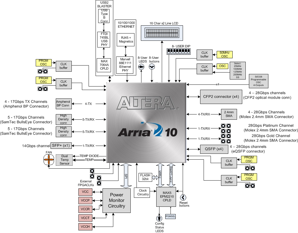
5.1. Board Overview
This section provides an overview of the Arria® 10 GX transceiver signal integrity development board, including an annotated board image and component descriptions.
Figure 3. Overview of the Arria® 10 GX Transceiver Signal Integrity Development Board Features
| Board Reference | Type | Description |
|---|---|---|
| Featured Devices | ||
| U51 | FPGA | Arria® 10 GX1150 FPGA (10AX115F1932C) |
| U32 | CPLD | MAX® V CPLD (5M2210ZF256), 256-pin BGA |
| General User Input and Output | ||
| D13–D20 | User LEDs (Green) | User LEDs (Green) |
| D21–D26 | MAX® V LEDs (Green) | MAX® V LEDs (Green) |
| S1–S12 | User push buttons | User push buttons |
| SW2, SW6 | User DIP switches | User DIP switches |
| SW3 | MAX® V DIP Switch | MAX® V DIP Switch |
| J20 | LCD Display header | Connector for 16 character × 2 line LCD I2C |
| Configuration, Status and Setup Elements | ||
| J66 | Intel® FPGA Download Cable programming header (uses JTAG mode only) | Header to interface external Intel® FPGA Download Cable direct to FPGA (through USB2 MAX2) |
| D4 | Green LED | USB2 Transmit-Receive Activity |
| D8–D12 | Ethernet LEDs | Ethernet LEDs (TX/RX/LINK) |
| Clock Circuitry | ||
| X3 | 25-MHz oscillator | This 25-MHz oscillator is the clock source to clock buffer ICS557-03 that provides selectable frequencies and spread percentages of its differential outputs. |
| X4 | 50-MHz oscillator | This 50-MHz oscillator is the clock source to clock buffer SL18860DC that provides three 50 MHz outputs to the FPGA (×2) and the MAX® V (×1) |
| SW4 | Spread spectrum / frequency selection switch | SW4 selects frequency and spread spectrum percentages of clock buffer outputs ICS557-03. Refer to the SW-4 Board Reference table for additional details. |
| J49–J50 | External core clock input | SMA External input at CLKIN_3B0 p/n |
| J51–J52 | External core clock output | SMA external output at PLL_3B_CLKOUT0 p/n |
| Y3 | Transceiver dedicated reference clock / programmable oscillator | Feeds REFCLKs on left side of the Arria® 10 GX device and an LVDS trigger output at board reference J100/J101. The external input is available at board reference J53 and J54. The default frequency is 644.53125 MHz. |
| Y4 | Transceiver dedicated reference clock / programmable oscillator | Feeds REFCLKs on left side of the Arria® 10 GX device and an LVDS trigger output at board reference J102/J103. The external input is available at board reference J56 and J57. The default frequency is 706.25 MHz. |
| Y5 | Transceiver dedicated reference clock / programmable oscillator | Feeds REFCLKs on right side of the Arria® 10 GX device and an LVDS trigger output at board reference J104/J105. The external input is available at board reference J59 and J60. The default frequency is 625 MHz. |
| Y6 | Transceiver dedicated reference clock / programmable oscillator | Feeds REFCLKs on right side of the Arria® 10 GX device and an LVDS trigger an output at board reference J106/J107. The external input is available at board reference J62 and J63. The default frequency is 875 MHz. |
| Y2 | Global clock / 25 MHz oscillator | 25-MHz crystal oscillator input to Si5338A clock buffer that feeds core fabric |
| X5 | Global clock / 125 MHz oscillator | Feeds core fabric at CLKIN_2L0 p/n |
| Transceiver Interfaces | ||
| J46 | High density connector | 15 Gbps, 5 channels high density connector |
| J47 | High density connector | 15 Gbps, 5 channels high density connector |
J30–J45 J67–J74 |
2.4 mm SMA connector | 25.78 Gbps, 4 channels 2.4 mm SMA connector |
| J24 | CFP2 optical transceiver interface | 25.78 Gbps, 4 transceiver channels connected to the CFP2 module |
| J23, J25, J26, J27 | CFP2 optional MCLK input/output | CFP2 Tx MCLK SMA connectors CFP2 Rx MCLK SMA connectors |
| J28 | QSFP+ optical transceiver interface | 25.78 Gbps, 4 transceiver channels connected to the QSFP+ module |
| J29 | SFP+ optical transceiver interface | 14 Gbps, single transceiver channel connected to the SFP+ module. |
| J22 | Backplane connector | 17 Gbps, 4 transceiver channels connected to the Amphenol backplane connector |
| Memory Devices | ||
| U33, U34 | Flash memory | Two 1-Gbit Micron PC28F00AP30BF CFI flash device |
| Communication Ports | ||
| J19 | Gigabit Ethernet port | RJ-45 connector which provides a 10/100/1000 Ethernet connection through a Marvell 88E1111 PHY |
| CN1 | USB Type-B connector | Connects a type-B USB cable |
| Power Supply | ||
| U209 | LTM 2987 | Linear Technology Power monitor device |
| U225 | LTC2974 | Linear Technology Power monitor device |
| Board Reference Spread Spectrum/ Frequency Selection Switch | Spread Spectrum Buffer Inputs | ||||||||||||||||
|---|---|---|---|---|---|---|---|---|---|---|---|---|---|---|---|---|---|
| SW4-1 | S0 |
|
|||||||||||||||
| SW4-2 | S1 | ||||||||||||||||
| SW4-3 | SS0 |
|
|||||||||||||||
| SW4-4 | SS1 |