Arria® 10 GX Transceiver Signal Integrity Development Kit User Guide
ID
683553
Date
12/01/2025
Public
1. About This Development Kit
2. Getting Started
3. Development Board Setup
4. Board Update Portal
5. Board Components
6. Board Test System
7. Document Revision History for the Arria® 10 GX Transceiver Signal Integrity Development Kit User Guide
A. Programming the Flash Memory Device
B. Safety and Regulatory Compliance Information
A.1. CFI Flash Memory Map
A.2. Preparing Design Files for Flash Programming
A.3. Creating Flash Files Using the Nios® II EDS
A.4. Programming Flash Memory Using the Board Update Portal
A.5. Programming Flash Memory Using the Nios II EDS
A.6. Restoring the Flash Device to the Factory Settings
A.7. Restoring the MAX® V CPLD to the Factory Settings
6.4.9. Clock Control
The Clock Control application sets the Si570 programmable oscillators to any frequency between 10 MHz and 945 MHz and select frequencies to 1,400 MHz. The oscillator drives a 2-to-6 buffer that drives a copy of the clock to all transceiver blocks of the FPGA.
The Clock Control application runs as a stand-alone application. ClockControl.exe resides in the <package dir>\examples\board_test_system directory.
The Clock Control communicates with the MAX® V device on the board through the JTAG bus. The Si570 programmable oscillator is connected to the MAX® V device through a 2-wire serial bus.
Figure 25. The Clock Control
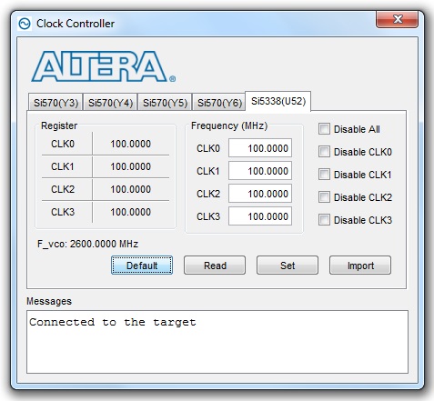
The following sections describe the Clock Control controls.