Arria® 10 GX Transceiver Signal Integrity Development Kit User Guide
ID
683553
Date
12/01/2025
Public
1. About This Development Kit
2. Getting Started
3. Development Board Setup
4. Board Update Portal
5. Board Components
6. Board Test System
7. Document Revision History for the Arria® 10 GX Transceiver Signal Integrity Development Kit User Guide
A. Programming the Flash Memory Device
B. Safety and Regulatory Compliance Information
A.1. CFI Flash Memory Map
A.2. Preparing Design Files for Flash Programming
A.3. Creating Flash Files Using the Nios® II EDS
A.4. Programming Flash Memory Using the Board Update Portal
A.5. Programming Flash Memory Using the Nios II EDS
A.6. Restoring the Flash Device to the Factory Settings
A.7. Restoring the MAX® V CPLD to the Factory Settings
6.4.1. The Configure Menu
Use the Configure menu to select the design you want to use. Each design example tests different functionality that corresponds to one or more application tabs.
Figure 16. The Configure Menu
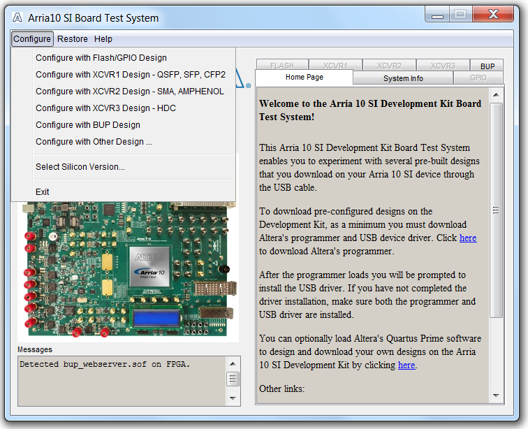
To configure the FPGA with a test system design, perform the following steps:
- On the Configure menu, click the configure command that corresponds to the functionality you wish to test.
- In the dialog box that appears, click Configure to download the corresponding design's SRAM Object File (.sof) to the FPGA. The download process usually takes less than a minute.
When configuration finishes, the design begins running in the FPGA. The corresponding GUI application tabs that interface with the design are now enabled. If you use the Quartus® Prime Programmer for configuration, rather than the Board Test System GUI, you may need to restart the GUI.