AN 957: Time-Sensitive Networking for Drive-on-Chip Design Example
ID
683707
Date
10/30/2021
Public
1. About the Time-Sensitive Networking for Drive-on-Chip Design Example
2. Getting Started with the TSN for Drive-on-Chip Design Example
3. Porting the Intel MAX 10 Drive-On-Chip design to the Cyclone V SoC Development Board
4. Running HPS Software for the TSN Drive-on-Chip Design
5. Connecting the Cyclone V SoC Development board to the Tandem 48 V Motion-Power board
6. Running the Program
7. TSN Configuration Example
8. Document Revision History for AN 957: Time-Sensitive Networking for Drive-on-Chip Design Example
A. Example .qsf for Pin Assignments and Attributes
B. Top-level Verilog HDL File Example
C. YOCTO Build Patch File (cvsx_doc_tsn_2_3-rt) for the TSN Drive-on-Chip Design Example
D. Script to read and change MAC addresses from Cyclone V SoC EEPROM
2.1. Hardware Requirements for the TSN for Drive-on-Chip Design Example
2.2. Software Requirements for the TSN for Drive-on-Chip Design Example
2.3. Configuring the Cyclone V SoC Development Board for the TSN for Drive-on-Chip Design Example
2.4. Programming the FPGA for the TSN for Drive-on-Chip Design Example
2.5. Creating an SD Card Image for the TSN for Drive-on-Chip Design Example
2.6. Turning on the Cyclone V SoC Development Board for the TSN for Drive-on-Chip Design Example
2.7. Configuring the TSN IP
3.1. Changing File Names, Revision Name, and Target Device for the TSN Drive-on-Chip Design Example
3.2. Modifying the Drive-On-Chip Qsys System
3.3. Adding the TTTech TSN IP to the Qsys system
3.4. Connecting the TSN and Drive-on-Chip Subsystems
3.5. Compiling the Quartus Prime Design and Top-Level Module
3.6. Generating the Preloader
3.7. Generating a .jic file
3.8. Compiling the Drive-on-Chip Design Software in Nios II Software Build Tools
3.9. Launching a YOCTO Build
3.10. Building an SD Card Image for the TSN Drive-on-Chip Design Example
3.11. Changing MAC Addresses
3.12. Reading and Checking Physical Addresses on the Cyclone V SoC Development Board
3.2. Modifying the Drive-On-Chip Qsys System
Several blocks in the Qsys system are not compatible with the Cyclone V SoC and you must delete or modify them.
- In Intel Quartus Prime, open the .qpf file by selecting File > Open Project.
- Open Qsys by selecting Tools > Qsys.
- In Qsys, select DOC_TANDEM_CVSX_NIOS_TSN_QSYS.qsys..
- Remove the blocks ADC_Trigger_master_0 and max10_adc.
These two blocks are for the Intel MAX 10 Development board and are not required for the implementation in Cyclone V SoC Development board.
- Remove the blocks ecfs_doc_threshold_sink, ALU_FOC_Float_av, and ALU_FOC_Fixp_av.
The design does not need these blocks and removing them frees up resources.
- Replace the blocks pll and pll2 as the module Avalon ALTPLL is not compatible with Cyclone V SoCs.
- Add the Altera PLL block and configure the PLL with the following settings:
Table 3. Altera PLL Settings Setting Value PLL mode Integer N-PLL Reference Clock Frequency 50.0 MHz Enable locked output port True Number of clocks 6 outclock0 Desired Frequency: 10.0 MHz
Phase shift: 0 ps
Duty Cycle: 50 %
outclock1 Desired Frequency: 10.0 MHz
Phase shift: 0 ps
Duty Cycle: 50 %
outclock2 Desired Frequency: 100.0 MHz
Phase shift: 0 ps
Duty Cycle: 50 %
outclock3 Desired Frequency: 20.0 MHz
Phase shift: 0 ps
Duty Cycle: 50 %
outclock4 Desired Frequency: 20.0 MHz
Phase shift: 10000 ps
Duty Cycle: 50 %
outclock5 Desired Frequency: 25.0 MHz
Phase shift: 0 ps
Duty Cycle: 50 %
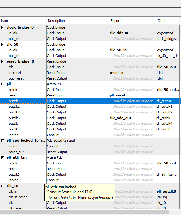
- Optionally, connect the new outputs of the PLL to clock source modules to ease the connection of the different clocks to other components.
Figure 6. Example for outclock0 to distribute clock signals
- Optional modifications):
- Remove the block named mm_bridge_0 and connect its secondaries (fast_periph_pb, lvmc_dclink, drive0, drive1) directly to the Avalon data master of the Nios II soft-processor and the JTAG master module
- Remove the block peripheral_pb and connect its secondaries (sys_console_debug_ram and periph_cbb) to Avalon data master of the Nios II soft-processor and the JTAG master module
- To boot-up the Nios II soft-processor from On-Board EPCQ memory, add an instance of Altera Serial Flash Controller and label it as epcq.
- Use the 25 MHz clock and connect it to the periph_cbb block.
- Connect the interrupt sender port to the irq port of the Nios II soft processor.
- Give the interrupt the number 4 and assign the addresses 0x0000_0100 to avl_csr and 0x0200_0000 to avl_mem ports.
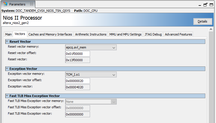
- For the Nios II soft processor to boot from on-board EPCQ memory, set up the Reset Vector in the Nios II Processor Settings.
Figure 7. Nios II Processor Reset Vector Settings
- Remove the block mem_if_ddr3_emif_0 and add it again. The previous external memory interface (EMIF) is exclusive to Intel MAX 10 devices. By removing and adding it again the new EMIF is for Cyclone V SoCs.
- Configure the EMIF.
Figure 8. DDR3 SDRAM Settings
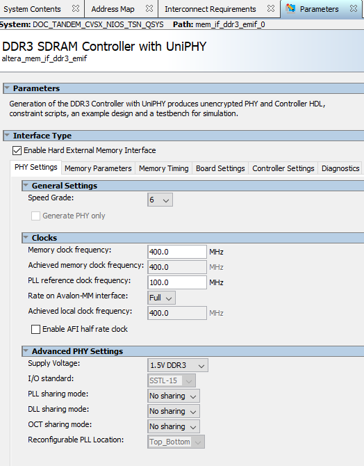 Figure 9. DDR3 SDRAM Settings
 Figure 10. DDR3 SDRAM Settings
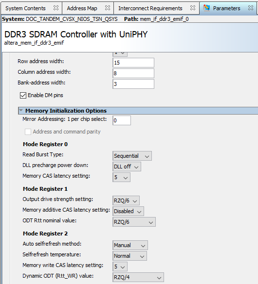 Figure 11. DDR3 SDRAM Settings
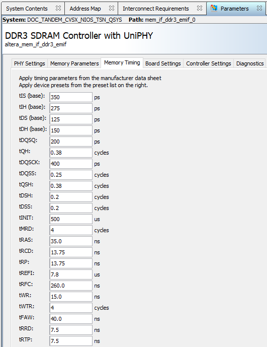 Figure 12. DDR3 SDRAM Settings
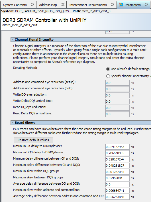 Figure 13. DDR3 SDRAM Settings
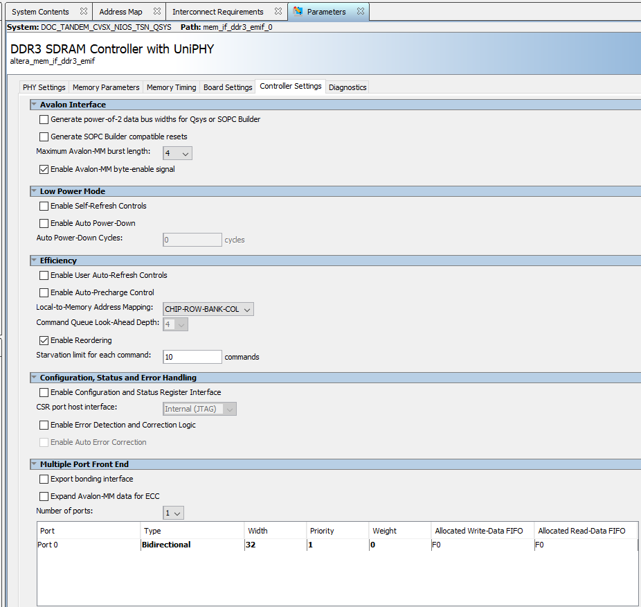 Figure 14. DDR3 SDRAM Settings
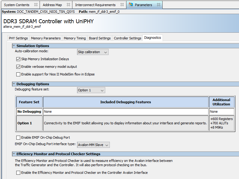
- Set the address assignment and interrupt enumeration.
Table 4. Address Interrupt and Enumeration Module Name Port Address Base and Interrupt Number DOC_CPU debug_mem_slave 0x0030_0000 irq IRQ0 TMC_I s1 0x0000_4000 s2 0x0000_4000 mem_if_ddr3_emif_0 avl_0 0x2000_0000 fast_periph_pb s0 0x0100_0000 performance_counter_0 control_slave 0x0000 doc_tmr_0 s1 0x0040 irq 2 doc_tmr_1 s1 0x0080 irq 3 jtag_uart avalon_jtag_slave 0x00c0 irq 1 lvmc_dclink lvdcdc_avs 0x0400_5000 drive0 drive_bridge_avs 0x0400_8000 doc_adc_irq 0 drive1 drive_bridge_avs 0x0400_c000 sys_console_debug_ram s1 0x0400_1000 s2 0x0400_1000 periph_ccb s0 0x1000_0000 sysid_0 control_slave 0x0000_0000 System ID 0x005046fe IO_IN_Buttons s1 0x0000_0020 IO_OUT_LED s1 0x0000_0040 gate_drive_spi spi_control_port 0x0000_0060 encoder_select s1 0x0000_0080 epcq avl_csr 0x0000_0100 avl_mem 0x0200_0000 interrupt_sender 4
The TSN drive-on-chip design is now integrated in the Qsys system. you can generate the hardware and instantiate it in the top-level Verilog HDL. You can add new high-level pin assignments to the system (refer to Example .qsf for Pin Assignments and Attributes)