AN 957: Time-Sensitive Networking for Drive-on-Chip Design Example
ID
683707
Date
10/30/2021
Public
1. About the Time-Sensitive Networking for Drive-on-Chip Design Example
2. Getting Started with the TSN for Drive-on-Chip Design Example
3. Porting the Intel MAX 10 Drive-On-Chip design to the Cyclone V SoC Development Board
4. Running HPS Software for the TSN Drive-on-Chip Design
5. Connecting the Cyclone V SoC Development board to the Tandem 48 V Motion-Power board
6. Running the Program
7. TSN Configuration Example
8. Document Revision History for AN 957: Time-Sensitive Networking for Drive-on-Chip Design Example
A. Example .qsf for Pin Assignments and Attributes
B. Top-level Verilog HDL File Example
C. YOCTO Build Patch File (cvsx_doc_tsn_2_3-rt) for the TSN Drive-on-Chip Design Example
D. Script to read and change MAC addresses from Cyclone V SoC EEPROM
2.1. Hardware Requirements for the TSN for Drive-on-Chip Design Example
2.2. Software Requirements for the TSN for Drive-on-Chip Design Example
2.3. Configuring the Cyclone V SoC Development Board for the TSN for Drive-on-Chip Design Example
2.4. Programming the FPGA for the TSN for Drive-on-Chip Design Example
2.5. Creating an SD Card Image for the TSN for Drive-on-Chip Design Example
2.6. Turning on the Cyclone V SoC Development Board for the TSN for Drive-on-Chip Design Example
2.7. Configuring the TSN IP
3.1. Changing File Names, Revision Name, and Target Device for the TSN Drive-on-Chip Design Example
3.2. Modifying the Drive-On-Chip Qsys System
3.3. Adding the TTTech TSN IP to the Qsys system
3.4. Connecting the TSN and Drive-on-Chip Subsystems
3.5. Compiling the Quartus Prime Design and Top-Level Module
3.6. Generating the Preloader
3.7. Generating a .jic file
3.8. Compiling the Drive-on-Chip Design Software in Nios II Software Build Tools
3.9. Launching a YOCTO Build
3.10. Building an SD Card Image for the TSN Drive-on-Chip Design Example
3.11. Changing MAC Addresses
3.12. Reading and Checking Physical Addresses on the Cyclone V SoC Development Board
3.3. Adding the TTTech TSN IP to the Qsys system
You build the TSN system within the TSN drive-on-chip design based on TTTech TSN IP.
- Copy the directory ip-sol-scv-release-2.3.0-30_03_2021\de_ip_solution_scv to <Quartus_Project>/ip and ip-sol-scv-release-2.3.0-30_03_2021\de-eval-board\fpga\misc_ip to <Quartus_Project>/ip.
- In Qsys, click Tools > Options and add the newly copied directories to the IP search paths.
Qsys automatically adds the TTTech IP to the IP catalog in the left upper corner of Qsys.Figure 15. TTTech TSN IP in IP Catalog
- Navigate to ip-sol-scv-release-2.3.0-30_03_2021\de-eval-board\fpga and open de-eval_scv.qar with Intel Quartus Prime.
The design opens including a Qsys system. The blocks in this design are identical to the ones in the TTTech Reference Design.
- In the Qsys system add the following functional blocks and connect them in the same way as the TTTech Reference Design.
Table 5. TSN subsystem blocks, addresses, and interrupts Module Name Description Port Address Base and Interrupt number hps_0 Arria V/ Cyclone V Hard Processor System f2h_sdram0_data 0x0000_0000 f2h_sdram1_data 0x0000_0000 f2h_ir10 IRQ 0 mm_bridge_0 Avalon-MM PipelineBridge s0 0x0000_0000 sys_qsys_0 System ID Peripheral control_slave 0x0001_0000 System ID 0x1c7e0004 rev_id_0 Internal Revision ID s 0x0004_0500 QSYS_SVM_ID 165499264 pio_0 PIO (Parallel I/O) s1 0x000f_0f00 eth_mdio_tristate_0 Altera’s Ethernet MDIO master with tristate logic csr 0x000f_0200 de_ip_solution_csv_0 DE-IP Solution SCV s_deip 0x0200_0000 irq0-ir115 0-15 - Connect the TSN blocks with a 100 MHz clock from the drive-on-chip subsystem.
- Add another Altera PLL block with the same 50 MHz reference clock as input (the same reference clock as the PLL for the drive-on-chip subsystem)
This additional 125 MHz clock is for the TSN IP m_dma_0_clk port.
- Configure the TSN IP with these parameters:
- Generics: BUS_CDC 0, FES_PORT_HIGH 2, BUFFER_SIZE 0, SCHEDULED_PORTS 31, PREEMPTABLE_PORTS 30, FRER_PORTS 31
- Options: LED_ACTIVE 0, Enable link LED interface (turn off)
- Adapters: Port 0 interface type DMA, Port 1 Interface Type MII, Port 2 Interface Type MII.
- Keep the multiple PIO blocks in the TTTech TSN IP Reference Design Qsys System and change the equivalent to pio_phy_reset (pio_0).
Keep the other PIO modules such as pio_led_debug, pio_pps_debug_out and pio_pps_debug_in.
- Configure the HPS module, even though the HPS and the secondary modules are connected in the same way as the TTTech TSN IP Reference Design Qsys system.
The HPS within the Cyclone V SoC Development board is connected to a different DDR3 memory than the TTTech Reference Board.Figure 16. HPS Settings
 Figure 17. HPS Settings
 Figure 18. HPS Settings
 Figure 19. HPS Settings
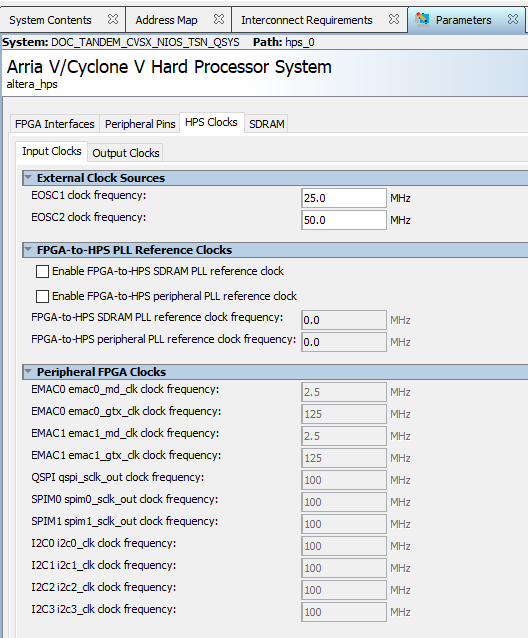 Figure 20. HPS Settings
 Figure 21. HPS Settings
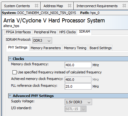 Figure 22. HPS Settings
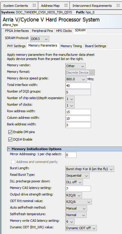 Figure 23. HPS Settings
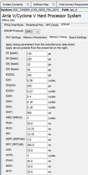 Figure 24. HPS Settings
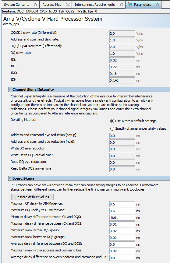
Both the drive-on-chip and TSN subsystems now work separately.