3.3.6. Custom Bridge Interfaces
Many bus protocols can be mapped to the system interconnect fabric either directly or with some custom bridge interface logic to compensate for differences between the interface standards. The Avalon® -MM interface standard, which Platform Designer supports, is a synchronous, memory-mapped interface that is easy to create custom bridges for.
If required, you can use the component editor available in Platform Designer to quickly define a custom bridge component to adapt the external processor bus to the Avalon® -MM interface or any other standard interface that is defined in the Avalon® Interfaces Specifications. The Templates menu available in the component editor includes menu items to add any of the standard Avalon® interfaces to your custom bridge. You can then use the Interfaces tab of the component editor to modify timing parameters including: Setup, Read Wait, Write Wait, and Hold timing parameters, if required.
For more information about the component editor, refer to the Creating Platform Designer Components chapter of the Intel® Quartus® Prime Handbook Volume 1: Design and Synthesis.
The Avalon® -MM protocol requires that all masters provide byte addresses. Consequently, it may be necessary for your custom bridge component to add address wires when translating from the external processor bus interface to the Avalon® -MM interface. For example, if your processor bus has a 16-bit word address, you must add one additional low-order address bit. If processor bus drives 32-bit word addresses, you must add two additional, low-order address bits. In both cases, the extra bits should be tied to 0. The external processor accesses individual byte lanes using the byte enable signals.
Consider the following points when designing a custom bridge to interface between an external processor and the Avalon® -MM interface:
- The processor bus signals must comply or be adapted with logic to comply with the signals used for transactions, as described in the Avalon® Interfaces Specifications.
- The external processor must support the Avalon® waitrequest signal that inserts wait-state cycles for slave components
- The system bus must have a bus reference clock to drive Platform Designer interface logic in the FPGA.
- No time-out mechanism is available if you are using the Avalon® -MM interface.
- You must analyze the timing requirements of the system. You should perform a timing analysis to guarantee that all synchronous timing requirements for the external processor and Avalon® -MM interface are met. Examine the following timing characteristics:
- Data tSU, tH , and tCO times to the bus reference clock
- fMAX of the system matches the performance of the bus reference clock
- Turn-around time for a read-to-write transfer or a write-to-read transfer for the processor is well understood
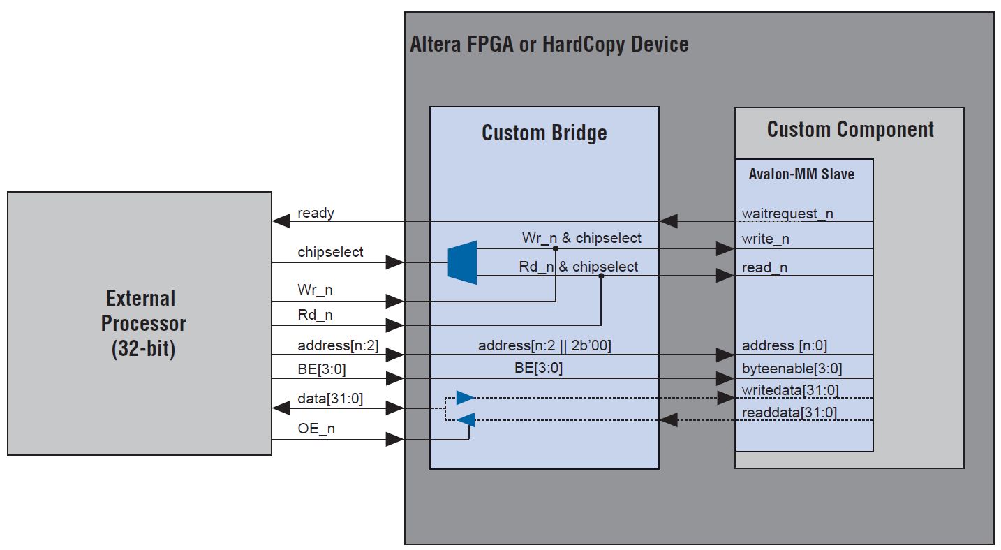
If your processor has dedicated read and write buses, you can map them to the Avalon® -MM readdata and writedata signals. If your processor uses a bidirectional data bus, the bridge component can implement the tristate logic controlled by the processor’s output enable signal to merge the readdata and writedata signals into a bidirectional data bus at the pins of the FPGA. Most of the other processor signals can pass through the bridge component if they adhere to the Avalon® -MM protocol. The figure below illustrates the use of a bridge component with a 32-bit external processor.
For more information about designing with the Avalon® -MM interface refer to the Avalon® Interfaces Specifications.