5.2.3.3.15.2.3.4.1. Hardware Design5.2.3.3.15.2.3.4.1. Hardware Design
The following sections describe a step-by-step method for building a bootable system for a Nios® II processor application executing in place from EPCQ flash.
IP Component Settings
- Create your Intel® Quartus® Prime and Platform Designer project.
- Add the Intel FPGA Serial Flash Controller IP to your Platform Designer system. Refer to the diagram below for the IP connection in Platform Designer.
Figure 87. Figure 99. Intel FPGA Serial Flash Controller IP Connections in Platform Designer
- The maximum input clock for Intel FPGA Serial Flash Controller IP is 25 MHz. The input clock must not exceed this maximum value.
- Both Intel FPGA Serial Flash Controller and Intel FPGA Serial Flash Controller II are designed to support Intel EPCQ devices. Intel FPGA Serial Flash Controller II is the newest version and supports higher performance. Intel recommends to use the Intel FPGA Serial Flash Controller II for your new designs.
Reset and Exception Vector Settings for Nios II Execute-In-Place
- Under Reset Vector in the Vectors tab, select EPCQ (epcq_controller_0.avl_mem) in the Reset vector memory drop-down menu and type the reset vector offset in the Reset vector offset entry box. The reset vector must be the base address of your application. In this example, it is 0x01E00000.
Note:
Your *.sof image size influences your reset vector offset configuration. The reset vector offset is the start address of the .hex file in EPCQ flash and it must point to a location after the *.sof image. You can determine the minimum reset vector offset by using the following equation:
minimum reset vector offset= (.sof image start address + .sof image size) in HEX
For example, if your *.sof image starts at address 0x0 and is 512 KB in size, then the minimum reset vector offset location you can select is 0x0080000. If the *.sof image space and the reset vector offset location overlap, Intel® Quartus® Prime software displays an overlap error.
- Under Exception Vector, you may select EPCQ (epcq_controller_0.avl_mem) or OCRAM in the Exception vector memory drop-down menu. In this example, 0x20 is listed for the Exception vector offset entry.
Note: When executing-in-place, the Nios® II processor boots and runs directly from EPCQ flash, without copying any code at boot time. Because the Nios® II begins executing at the reset address in this case, exception vectors must be located at a nonzero exception vector offset to allow for instructions between the reset vector and the base of the exception vectors. Thus, you must include an exception vector offset when the reset vector and the exception vector point to the same memory and no boot copier is present.Figure 88. Figure 100. Exception Vector Settings in Platform Designer
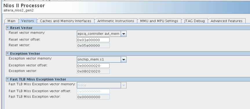 Note: Intel FPGA recommends setting the exception vector to OCRAM to make the interrupt processing faster.
 - Click Finish. You will return to the Platform Designer System Contents tab.
- Double-click on the Intel FPGA Serial Flash Controller IP to open the Intel FPGA Serial Flash Controller Parameter editor.
- Select the Configuration device type based on your hardware design and choose the desired I/O mode.
- Close the Parameter Editor and return to the Platform Designer System Contents tab.
- Click Generate HDL to generate your Platform Designer design.
- Compile your design in Intel® Quartus® Prime software.
Intel Quartus Prime Software Settings
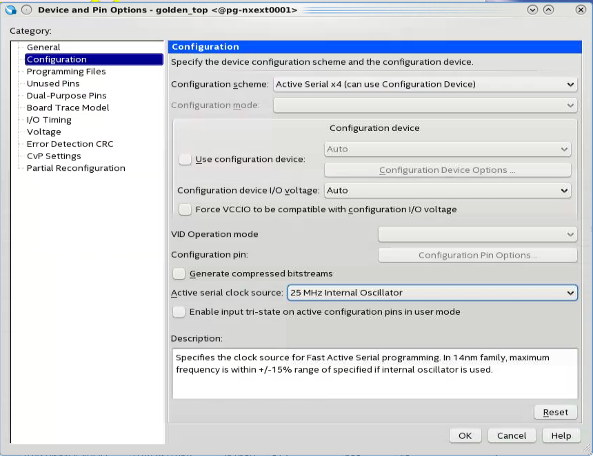
- In the Intel® Quartus® Prime software, click on Assignment > Device > Device and Pin Options > Configuration.
- Set Configuration scheme to Active Serial x4 (can use Configuration Device).
- Set the Active serial clock source to 25 MHz Internal Oscillator.