Intel® Quartus® Prime Standard Edition User Guide: PCB Design Tools
1.3. Understanding SSN
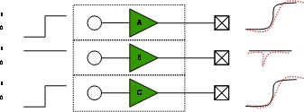
In a sample system with three pins, two of the pins (A and C) are switching, while one pin (B) is quiet. If the pins are driven in isolation, the voltage waveforms at the output of the buffers appear without noise interference, as shown by the solid curves at the left of the figure. However, when pins A and C are switching simultaneously, the noise generated by the switching is injected onto other pins. This noise manifests itself as a voltage noise on pin B and timing noise on pins A and C.
Voltage noise is measured as the change in voltage of a signal due to SSN. When a signal is QH, it is measured as the change in voltage toward 0 V. When a signal is QL, it is measured as the change in voltage toward VCC.
In the Intel® Quartus® Prime software, only voltage noise is analyzed. Voltage noise can be caused by SSOs under two worst-case conditions:
- The victim pin is high and the aggressor pins (SSOs) are switching from low to high
- The victim pin is low and the aggressor pins (SSOs) are switching from high to low
SSN can occur in any system, but the induced noise does not always result in failures. Voltage functional errors are caused by SSN on quiet victim pins only when the voltage values on the quiet pins change by a large voltage that the logic listening to that signal reads a change in the logic value. For QH signals, a voltage functional error occurs when noise events cause the voltage to fall below VIH. Similarly, for QL signals, a voltage functional error occurs when noise events cause the voltage to rise above VIL. Because VIH and VIL of the Altera device are different for different I/O standards, and because signals have different quiet voltage values, the absolute amount of SSN, measured in volts, cannot be used to determine if a voltage failure occurs. Instead, to assess the level of impact by SSN in the SSN analysis, the Intel® Quartus® Prime software quantifies the SSN in terms of the percentage of signal margin in Intel devices.
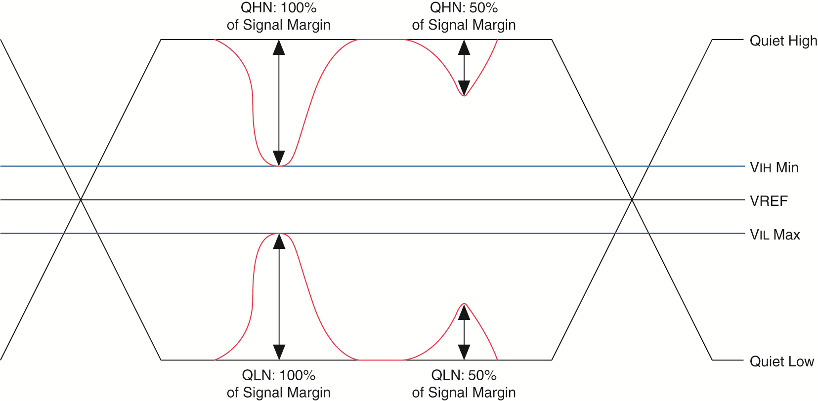
The figure shows four noise events, two on QH signals and two on QL signals. The two noise events on the right-side of the figure consume 50 percent of the signal margin and do not cause voltage functional errors. However, the two noise events on the left side of the figure consume 100 percent of the signal margin, which can cause a voltage functional error.
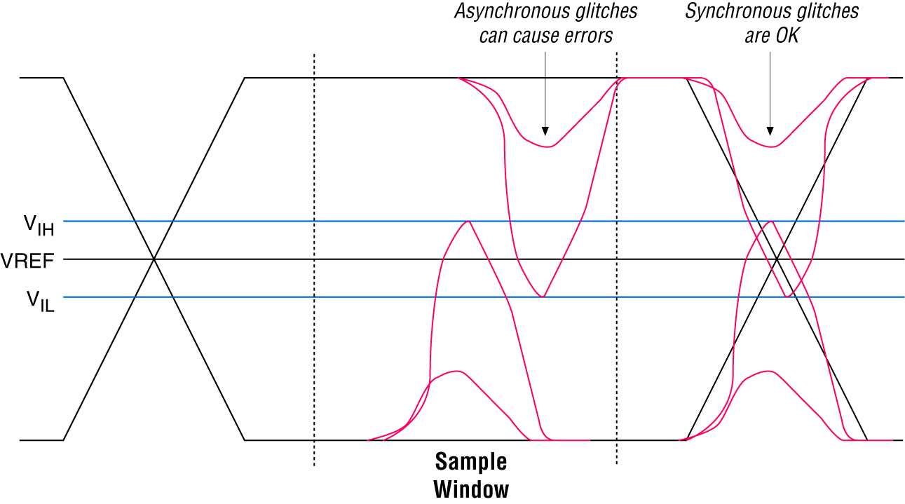
Noise caused by aggressor signals are synchronously related to the victim pin outside of the sampling window of a receiver. This noise affects the switching time of a victim pin, but are not considered an input threshold violation failure.