Intel® Quartus® Prime Standard Edition User Guide: PCB Design Tools
1.7. Optimizing Your Design for SSN Analysis
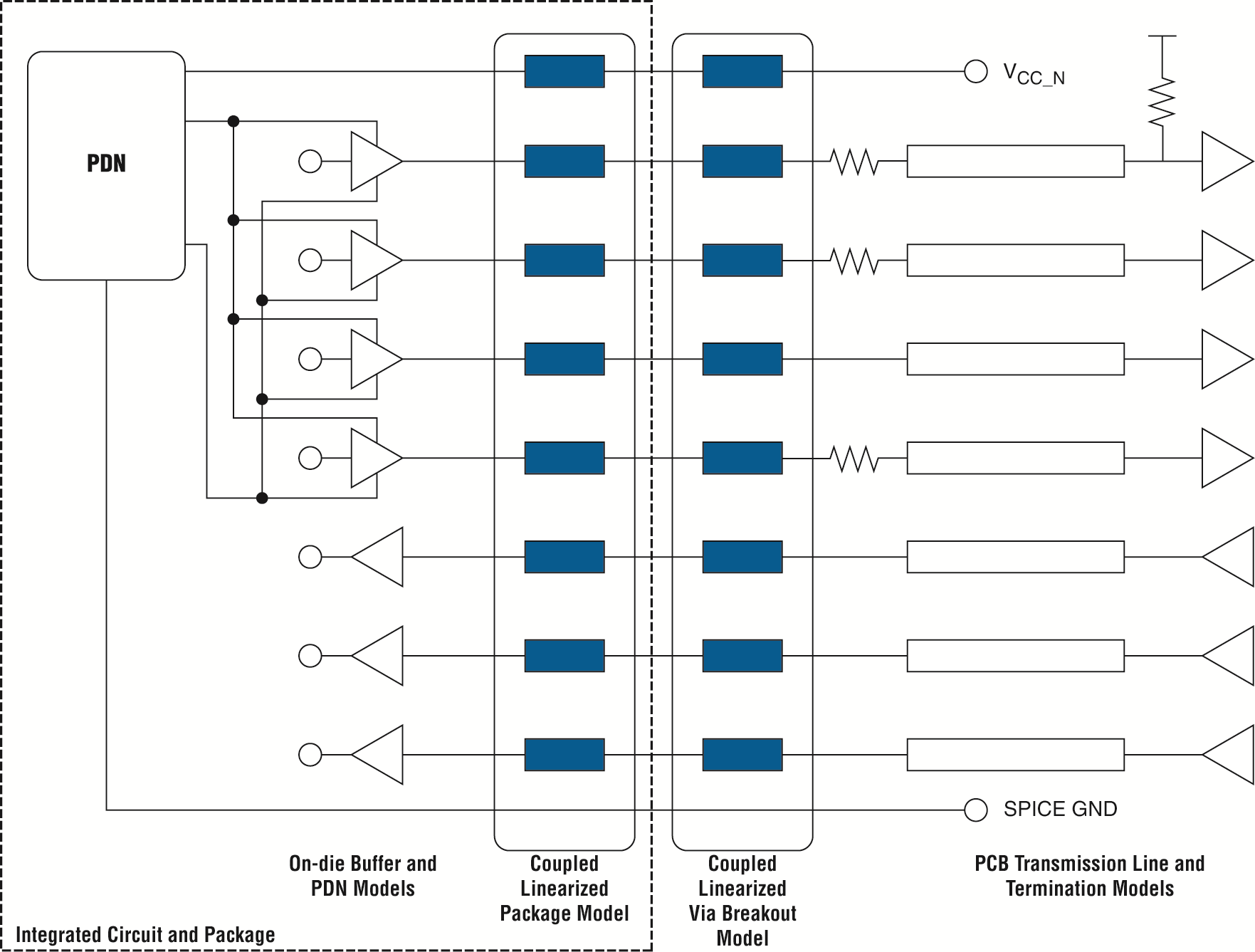
The SSN Analyzer produces a voltage noise estimate for each input, output, and bidirectional pin in the design. It allows you to estimate the SSN levels, comprised of QLN and QHN levels, for your FPGA pins. Performing SSN analysis helps you optimize your design for SSN during compilation.
Because the SSN Analyzer is integrated into the Intel® Quartus® Prime software, it can automatically set up a system topology that matches your design. The SSN Analyzer accounts for different I/O standards and slew rate settings for each buffer in the design and models different board traces for each signal. Also, it correctly models the state of the unused pins in the design. The SSN Analyzer leverages any custom board trace assignments you set up for use by the advanced I/O timing feature.
The SSN Analyzer also models the package and vias in the design. Models for the different packages that Altera devices support are integrated into the Intel® Quartus® Prime software. In the Intel® Quartus® Prime software, you can specify different layers on which signals break out, each with its own thickness, and then specify which signal breaks out on which layer.
After constructing the circuit topology, the SSN Analyzer uses a simulation-based methodology to determine the SSN for each victim pin in the design.