Video and Vision Processing Suite Intel® FPGA IP User Guide
A newer version of this document is available. Customers should click here to go to the newest version.
45.3. Video Frame Reader IP Functional Description
Configure the IP with the number of buffer sets you want to set up by programming the csr_num_buffer_sets register. For each set, program the number of buffers, the base address and buffer offsets, the buffer dimensions and colorspace information into the buffer set registers. Set the csr_buffer_mode register to multiple buffer sets mode, where the IP automatically reads buffers from the next set when the IP produces the last buffer from the current set. Otherwise, the IP reads buffers from the current set only. Program the csr_starting_buffer_set register and set the LSB of the csr_run register and the IP starts producing output frames as soon as you write to the csr_commit register.
If bit [1] of csr_run is set, this configures single-shot mode. In this mode the IP halts once the last buffer from a set has been output.
If you want to use an external timing synchronizing signal to time the output of the reads, set the csr_run register to 2. In this mode, configure the IP as usual but provide a rising or falling edge on the frame sync conduit when you want the IP to start outputting each frame.
If you want the IP to produce frames on a rising edge only, set csr_fsync_pulse_mode.
If a frame sync edge is detected while the IP is already outputting a frame, the IP starts outputting the next frame immediately following the current frame.
Set csr_run to 0 and write to the csr_commit register for the IP to stop at the end of the current frame.
Register Behavior
Bit [0] of the csr_status register goes high when the IP starts producing the first frame. It goes low after the IP finishes outputting the last line of the frame. It returns high when the IP starts producing the next frame.
The csr_last_buffer_read register updates with the base address of a frame when the IP finishes producing it.
Applications that need to know when the IP produces frames can poll these status registers. Alternatively, use the IRQ_CONTROL register to set up an interrupt when the IP finishes producing a frame.
Double-buffer applications
You can often use a double buffer for applications where a CPU or GPU (the host) is producing frames. The host writes to one buffer while the IP reads from the other buffer. When the host completes writing the new frame, the IP switches to read from the new frame. The host can then start creating the next frame in the buffer that the IP is no longer reading from.
To configure a double buffer using the IP, Intel recommends you configure two buffer sets, each with one buffer. Think of each buffer set as one buffer. The IP produces video first from one buffer, then the other, according to the csr_starting_buffer_set register.
Program the registers as follows:
- CSR_NUM_BUFFER_SETS = 2 (2 sets, each with 1 buffer)
- CSR_BUFFER_MODE = 0 (to prevent the IP automatically advancing to the buffer in set 1 before the host writes the new frame)
- CSR_STARTING_BUFFER_SET = 0 (the host creates the frame in set 0 first)
- CSR_RUN = 1 (the IP continuously produces all frames from the current set, in this case it is just one frame)
The buffer set registers at CSR_BUFFER_0_BASE and CSR_BUFFER_1_BASE must be programmed with the correct base addresses and other specifics for both buffers (refer to Buffer set register banks ).BUFFER_0_NUM_BUFFERS and BUFFER_1_NUM_BUFFERS must be set to 1, as each set only contains one buffer. With only one buffer in each set, the BUFFER_N_INTER_BUFFER_OFFSET register is unused.
When the host completes writing the first frame to CSR_BUFFER_0_BASE, write CSR_COMMIT = 1 and the IP starts producing this frame repeatedly.
The host can now start constructing a frame at CSR_BUFFER_1_BASE. When the host finishes, program:
- CSR_STARTING_BUFFER_SET = 1
- CSR_COMMIT = 1
The IP now produces repeatedly the new frame at CSR_BUFFER_1_BASE.
This process can now iterate, with the host writing at CSR_BUFFER_0_BASE again and instructing the IP to change to that frame:
- CSR_STARTING_BUFFER_SET = 0
- CSR_COMMIT = 1
Multivideo applications
You can establish multiple sets of buffers for multivideo applications. The host holds videos segments in memory and the IP can read any of the segments, with the option to advance automatically via the multiple buffer sets mode to the next segment.
For an example with five video segments, with segments available at base addresses CSR_BUFFER_0_BASE to CSR_BUFFER_4_BASE, for a display of all the sequences in turn, program the registers as follows:
- CSR_NUM_BUFFER_SETS = 5
- CSR_BUFFER_MODE = 1 (So the IP automatically advances to the first buffer in the next set after outputting the last buffer from the current set)
- CSR_STARTING_BUFFER_SET = 3 (Start the output from set 3 first)
Program the base addresses and other specifics for both buffers in register sets from CSR_BUFFER_0_BASE to CSR_BUFFER_4_BASE (refer to Buffer set register banks).
CSR_RUN = 1 (The IP continuously produces all frames from each set, before the buffer_mode setting moves it on to the next set)
CSR_BUFFER_N_NUM_BUFFERS is programmed with the correct number of frames for sequence N, for example 3600 for a one-minute video at 60 Hz.
Each set may have different resolutions and color spaces, but every buffer within each set must have the same resolution and color space.
Write CSR_COMMIT = 1 to commence output of all five video segments in turn.
To implement this 5 video segment example the host should manually establish when a set produces its final frame and dynamically configure the next set. However, using the in-built buffer set registers is more convenient and ensures multivideo playback continues even if the host cannot program the next set in time, for example when using a debugger.
Frame synced applications
Set CSR_RUN to 2 to enable frame synchronization. In this mode, set up the buffer sets as described earlier and the IP produces frames whenever it detects a frame sync edge on the fsync_in_read input.
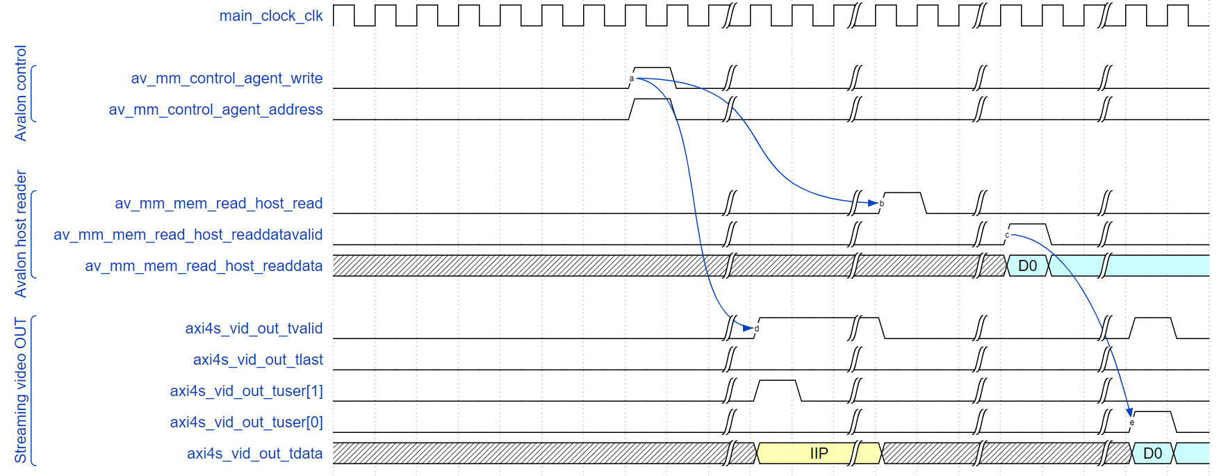
Latency
The frame reader latency depends on the availability of the external memory interfaces, which may create backpressure on the IP’s read interface via the av_mm_mem_read_host_waitrequest signal.
The streaming video output experiences backpressure via the axi4s_vid_out_tready input. The worst-case latency figures are for when the frame reader experiences no backpressure. Any backpressure increases these latencies by the same amount of cycles.
The latency figures are for when the host interfaces do not have a separate clock, so all interfaces operate from the same clock.
| Initiating event | Resultant event | Latency (measured in clock cycles) | Labels in figure |
|---|---|---|---|
| With csr_run register LSB previously set, a write to csr_commit | Image information packet (full mode only) | 10 | a->d |
| With csr_run register LSB previously set, a write to csr_commit | Read initiated by av_mm_mem_read_host_ read | 14 | a->b |
| av_mm_mem_read_host_readdatavalid strobe high to return the first frame data | axi4s_vid_out_tuser[0]strobe to indicate start of frame on streaming output | 20 | c->e |