Video and Vision Processing Suite Intel® FPGA IP User Guide
A newer version of this document is available. Customers should click here to go to the newest version.
41.3. Test Pattern Generator IP Functional Description
- Bars pattern
- Color bars
- Grayscale bars
- Black and white bars
- Mixed bars
- Constant color
- SDI pathological
- Zone plate
- Digital clock
Bars pattern
If you select Bars Pattern, the IP produces a test pattern with 8 vertical bars, each covering approximately 1/8th of each output video line. The bars contain either a sequence of changing colors (color bars), a sequence of greyscale tones with decreasing brightness (greyscale bars), or a sequence of alternating black and white bars. Mixed bars change the pattern in the vertical direction, with the first 1/8th of the lines showing the black and white bars, the next 1/8th showing the greyscale bars, and the final ¾ showing the color bars. If you select bars pattern (and turn on the Avalon memory-mapped control agent interface), a value in the register map selects at run time which variant of the bars pattern to display. If you do not turn on Avalon memory-mapped control agent, the fixed bars mode parameter controls which variant of the bars pattern to display, and you cannot change it at run time.
For all test patterns, each bar is approximately 1/8th of the width of the output frame, but this width is not exact. The actual width of each color bar is affected by the field width and the horizontal subsampling.
When the width of the field is not divisible by eight, the remainder pixels from the division are spread as evenly as possible across the bars. The first bar, on the left-hand side of the field, always has floor(field_width/8) pixels. A single remainder pixel is added to the width of each subsequent bar until all the remainder pixels are exhausted. The width of each bar cannot be less than the number of pixels transmitted per beat at the output interface (pixels in parallel). If the field width is set to less than 8 x pixels in parallel, as many bars as possible display with pixels in parallel pixels per bar, but fewer than 8 bars display. When the output is horizontally subsampled (4:2:2 or 4:2:0), the pixel-width of each color bar is a multiple of two and we alter the methods described above to ensure this is always the case.
The tables define the values of the color components in each bar for each of the three basic modes. The values are the actual output values if you set bits per color plane to 8 bits. If bits per color is greater than 8 bits, the internal logic upshifts the value by the required number of bits, with zeros added in the LSBs.
| Color | RGB | YCbCr |
| White (left) | (180, 180, 180) | (180, 128, 128) |
| Yellow | (180, 180, 16) | (162, 44, 142) |
| Cyan | (16, 180, 180) | (131, 156, 44) |
| Green | (16, 180, 16) | (112, 72, 58) |
| Magenta | (180, 16, 180) | (84, 184, 198) |
| Red | (180, 16, 16) | (65, 100, 212) |
| Blue | (16, 16, 180) | (35, 212, 114) |
| Black (right) | (16, 16, 16) | (16, 128, 128) |
| Color | RGB | YCbCr |
| 0 (left) | (180, 180, 180) | (180, 128, 128) |
| 1 | (162, 162, 162) | (162, 128, 128) |
| 2 | (131, 131, 131) | (131, 128, 128) |
| 3 | (112, 112, 112) | (112, 128, 128) |
| 4 | (84, 84, 84) | (84, 128, 128) |
| 5 | (65, 65, 65) | (65, 128, 128) |
| 6 | (35, 35, 35) | (35, 128, 128) |
| 7 (right) | (16, 16, 16) | (16, 128, 128) |
| Color | RGB | YCbCr |
| 0 (left) | (180, 180, 180) | (180, 128, 128) |
| 1 | (16, 16, 16) | (16, 128, 128) |
| 2 | (180, 180, 180) | (180, 128, 128) |
| 3 | (16, 16, 16) | (16, 128, 128) |
| 4 | (180, 180, 180) | (180, 128, 128) |
| 5 | (16, 16, 16) | (16, 128, 128) |
| 6 | (180, 180, 180) | (180, 128, 128) |
| 7 (right) | (16, 16, 16) | (16, 128, 128) |
Constant color
The constant color test pattern is a complete field or frame of a constant color. This test pattern has limited value for testing, but you can use the pattern to form a background layer for a mixer. Set the RGB or YCbCr values for the desired color as either fixed, compile-time-set parameters or run-time controlled values through the Avalon memory-mapped control agent interface.
SDI Pathological
The SDI pathological test pattern is specifically designed to stress test the SDI equalizer and PLL performance. The test pattern consists of a static test image with the top half of the lines filled with a shade of magenta, and the bottom half of the lines filled with a shade of gray.
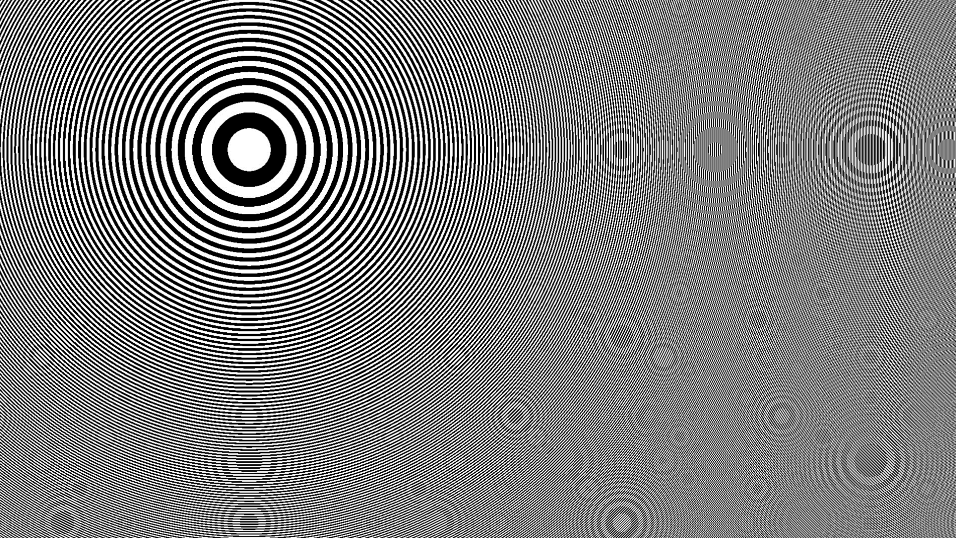
Zone plate
The zone plate test pattern is an arbitrarily sized, arbitrarily placed set of concentric rings that get wider and narrower the further from the origin. If Avalon memory-mapped control agent is off, the origin is always at the center of the display. If Avalon memory-mapped control agent is on, you can configure the origin by writing to the ZONE_X_ORIGIN and ZONE_Y_ORIGIN register map values.
Set the Coarse scaling coefficient bits in the ZONE_POWER_FACTOR register to set the initial size of the zone plate so that it is visible with the current resolution. Set the fine tune scaling coefficient bit in the ZONE_FINE_FACTOR register for incremental changes to the size that smoothly resize the plate. If Avalon memory-mapped control agent is on. you can configure these values by writing to the respective registers, otherwise these values are fixed at compile time.
Because of the position of k in the equation, increasing k causes a decrease in the size of the zone plate (decreased zoom). Increasing k causes an increase in the size of the zone plate (increased zoom).


Digital clock
The digital clock pattern consists of a digital display with format HH:MM:SS,FC, where FC is field count. The time is not precise but is a function of frames per second and field count.
You can customize the size of the display. The original dimensions of the display are 88x8 pixels. If Avalon memory-mapped control agent is on, the value of Fixed clock scale factor is a scalar multiple to both dimensions. If Avalon memory-mapped control agent is off, the value of the Scale factor bit in the CLOCK_SCALE_FACTOR register is a scalar multiple to both dimensions.
Set the background or font color and location at either compile time if Avalon memory-mapped control agent is off, or at run time via the register map.
Output subsampling and color space
You can configure the output subsampling and color space to either be fixed and set at compile time, or to be variable at run time using the Avalon memory-mapped control agent interface.
The Output Format parameter sets the subsampling option:
- 4:4:4. Output is fixed at full sampling for each color plane (can be RGB or YCbCr). Each pixel has 3 color planes.
- 4:2:2. Output is fixed at full sampling on the Y plane and horizontal subsampling on the Cb and Cr planes (RGB data is not supported in 4:2:2 mode). Each pixel has 2 color planes.
- 4:2:0. Output is fixed at full sampling on the Y plane and horizontal and vertical subsampling on the Cb and Cr planes (RGB data is not supported in 4:2:0 mode). Each pixel has 3 color planes.
- Monochrome. Output has only 1 color plane per pixel and represents only a fully sampled Y plane.
- Variable. Output can be configured at run time to be 4:4:4 RGB, 4:4:4 YCbCr, 4:2:2 YCbCr, or 4:2:0 YCbCr. Each pixel has 3 color planes.
The IP allows you to select up to 8 different test pattern configurations to switch between at run time:
- Each configuration is a combination of 1 of the 3 available patterns and a formatting option.
- Each test pattern configuration is fixed in one particular output format. However, by selecting between the patterns, you can vary the overall output format at run time.
For example, you may include 4 different configurations, all of which use the bars pattern, but with the first configuration set to 4:4:4 RGB, the second set to 4:4:4 YCbCr, the third set to 4:2:2 YCbCr, and the fourth set to 4:2:0 YCbCr. With this setting, you can validate all the possible configurations of an HDMI 2.0 output.
Updating settings at run time
If you turn on the Avalon memory-mapped control agent interface, the resolution, interlace settings and test pattern configuration can be adjusted at run time via the register map. The model for executing settings changes at run time differs depending on whether the test pattern generator is parameterized to output the full or lite variant of the Intel FPGA streaming video protocol.
Full Variants
When you turn off Lite mode, you can edit any of the test pattern generator settings at any time. The IP does not apply the settings until the start of the next frame after a write to the COMMIT register (address 0x014C). The IP can complete a change to the settings that requires writes to multiple registers without the risk of applying the earlier writes in the sequence one frame before the later writes in the sequence.
The full sequence for register updates for full variants is:
- Make the required edits to any subset of the test pattern generator settings in the register map (addresses 0x120 to 0x0128 and addresses 0x0150 and 0x015C to 0x0168).
- After the first write to update a setting, the IP asserts bit 1 of the STATUS register (address 0x0140) in the return data for any read to this address.
- Write any value to the COMMIT register (address 0x014C) to commit the changes as a coherent set.
- Do not make any further edits to the settings until the IP deasserts bit 1 of the STATUS register at the next field boundary after the write to the COMMIT register. If the IP has any updates to the test pattern settings (address 0x0120 to 0x0128, and 0x0150), at this point the field index is reset to 0. The field index is a count of the number of frames since the last update. The interlace sequence is reset to start at F0 or F1, as specified in the register map.
- When the IP deasserts bit 1 of the STATUS register, you may make further settings updates.
The COMMIT mode register gates the application of updates to all registers except the CONTROL register (address 0x0148). The CONTROL register allows you to stop and start the IP output at frame boundaries. The IP applies updates to the CONTROL register at the next field boundary, regardless of whether you write to the COMMIT register.
Lite mode
If you turn on Lite mode the IP has no COMMIT register functionality. The recommended flow for updating the test pattern generator settings is:
- Write 0 to the CONTROL register (address 0x0148) to stop the test pattern generator at the next field boundary.
- Read the STATUS register (address 0x0140) until bit 0 is de-asserted, indicating that the test pattern generator is in an idle state between fields.
- Make the required edits to any subset of the test pattern generator settings in the register map (addresses 0x120 to 0x0128 and addresses 0x0150 and 0x015C to 0x0168).
- Write 1 to the CONTROL register to restart the test pattern generator with the new settings. If the IP has any updates to the test pattern settings (address 0x0120 to 0x0128, and 0x0150), at this point the field index is reset to 0. The interlace sequence is reset to start at F0 or F1, as specified in the register map.