6.1. General DDR Signal Routing Guideline on PCB
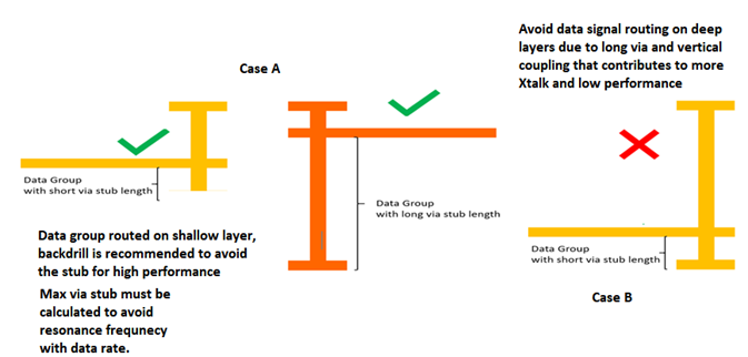
Route the data group signals (DQ, DM and DQS signals) on shallow layers—stripline or microstrip line. For better performance, use the shortest Z-height via transitions to avoid vertical crosstalk.
Long via stubs affects the channel ISI, however the impact of ISI is less than the impact of crosstalk for the maximum data rate performance.
To minimize horizontal crosstalk between signals on the same layer, Altera recommends maintaining adequate signal trace–to–trace (edge to edge) space. Keep a minimum spacing of 3× H2 separation distance for inner layer as shown in the following figure. Certain signals within the same group can have smaller spacing, such as DQ to DQ. For more details about the spacing requirement, refer to the respective routing guide sections for each signal group.

Section Content
FPGA DDR Break Out Routing
DRAM Break Out in Layout Routing
Ground Plane and Return Path