Multi Channel DMA Intel® FPGA IP for PCI Express* Design Example User Guide
ID
683517
Date
6/09/2025
Public
A newer version of this document is available. Customers should click here to go to the newest version.
3.5.1. Hardware Requirements
3.5.2. Software Requirements
3.5.3. Set Up the Hardware and Program the FPGA
3.5.4. Configuration Changes from BIOS
3.5.5. Host Operating System Check for Ubuntu v22.04
3.5.6. Installing the Required Kernel Version for Ubuntu v24.04
3.5.7. Set the Boot Parameters
3.5.8. MCDMA Custom Driver
3.5.9. MCDMA DPDK Poll Mode Driver
3.5.10. MCDMA Kernel Mode Network Device Driver
3.5.3. Set Up the Hardware and Program the FPGA
Note: This section describes how to program the FPGA using the Stratix® 10 Development Board. If you are using one of the boards listed in the previous section, the name of the development board you select shall apply for this section accordingly.
- Install the Stratix® 10 FPGA Development Kit into a PCIe Gen3 x16 slot on the host system, connected to the ATX 6-pin power supply.
- Connect the Stratix® 10 FPGA Development Board to a computer system in which the Quartus® Prime Pro Edition software is installed using the USB cable shipped along with the development kit for FPGA configuration.
- Power on the host system and turn on the power switch on the development kit.
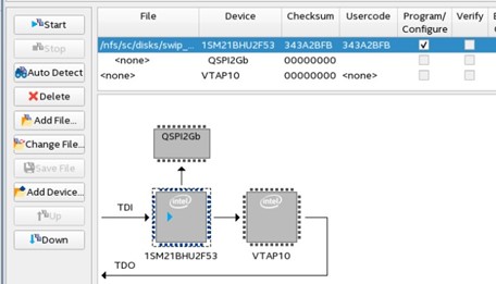
- In the Quartus® Prime Pro Edition software, invoke the programmer by clicking Tools > Programmer.
- In the Programmer, click Hardware Setup and verify the Stratix® 10 FPGA Development Kit is detected in the Hardware Setting tab. For Currently selected hardware, select the Stratix® 10 FPGA Development Kit and then click Close.
- Click Auto Detect to detect the JTAG device chain.
- Select the target FPGA device in the JTAG chain, select Change File, and select the pcie_ed.sof. Then, click Open.
- Check the Program/Configure option, and click Start to start the FPGA configuration.
Figure 30. Programming the Stratix® 10 MX FPGA Development Board
- Perform a warm reboot for the host system once the Stratix® 10 FPGA is successfully configured.
- Check the enumeration of the PCIe Endpoint device ( Stratix® 10 FPGA Development Kit) on the host system by running the lspci –d 1172: command in a Linux terminal.
Expected result:
BDF Unassigned class [ff00]: Altera Corporation Device 0000 (rev 01)