AN 894: Signal Tap Tutorial with Design Block Reuse: for Intel® Cyclone® 10 GX FPGA Development Board
ID
683454
Date
11/11/2019
Public
1. Introduction
2. Core Partition Reuse Debug—Developer
3. Core Partition Reuse Debug—Consumer
4. Root Partition Reuse Debug—Developer
5. Root Partition Reuse Debug—Consumer
6. Document Revision History for AN 894: Signal Tap Tutorial with Design Block Reuse for Intel® Cyclone® 10 GX FPGA Development Board
2.1. Step 1: Creating a Core Partition
2.2. Step 2: Creating Partition Boundary Ports
2.3. Step 3: Compiling and Checking Debug Nodes
2.4. Step 4: Exporting the Core Partition and Creating the Black Box File
2.5. Step 5: Copying Files to Consumer Project
2.6. Step 6: Creating a Signal Tap File (Optional)
2.7. Step 7: Programming the Device and Verifying the Hardware
2.8. Step 8: Verifying Hardware with Signal Tap
3.1. Step 1: Adding Files and Running Synthesis
3.2. Step 2: Creating a Signal Tap File
3.3. Step 3: Creating a Partition for blinking_led_top
3.4. Step 4: Compiling the Design and Verifying Debug Nodes
3.5. Step 5: Programming the Device and Verifying the Hardware
3.6. Step 6: Verifying Hardware with Signal Tap
4.1. Step 1: Creating a Reserved Core Partition and Defining a Logic Lock Region
4.2. Step 2: Generating and Instantiating SLD JTAG Bridge Agent in the Root Partition
4.3. Step 3: Generating and Instantiating the SLD JTAG Bridge Host
4.4. Step 4: Generating HDL Instance of Signal Tap
4.5. Step 5: Compiling Export Root Partition and Copying Files to Consumer Project
4.6. Step 6: Programming the Device and Verifying the Hardware
4.7. Step 7: Generating a Signal Tap File for the Root Partition
4.8. Step 8: Verifying the Hardware with Signal Tap
5.1. Step 1: Adding Files to Customer Project
5.2. Step 2: Generating and Instantiating SLD JTAG Bridge Host in Reserved Core Partition
5.3. Step 3: Synthesizing, Creating Signal Tap File, and Compiling
5.4. Step 4: Programming the Device and Verifying the Hardware
5.5. Step 5: Verifying the Hardware of Reserved Core Partition with Signal Tap
5.6. Step 6: Verifying Hardware of Root Partition with Signal Tap
4.8. Step 8: Verifying the Hardware with Signal Tap
- In the Signal Tap window, click File > Open, and open the stp_root_partition.stp file, which you created in the previous step.
- Ensure that the development kit is powered ON and connected to the machine from which you open the Signal Tap logic analyzer.
- Set up the JTAG Chain Configuration, and ensure Instance Manager is Ready to acquire.
- Verify that Bridge Index is set to None Detected in the JTAG Chain Configuration window.
Figure 34. JTAG Chain Configuration
- To set the trigger condition, select the count[0], count[1], count[2], and count[3] signals, right-click the column under Trigger Conditions, and select Falling Edge.
Figure 35. Trigger Conditions
- Run analysis by clicking Processing > Run Analysis.
When the analysis finishes, the Waveform tab shows the captured data.
- Verify the transition of the nodes in the root partition.
Figure 36. Waveforms for Root Partition Nodes in Developer Project
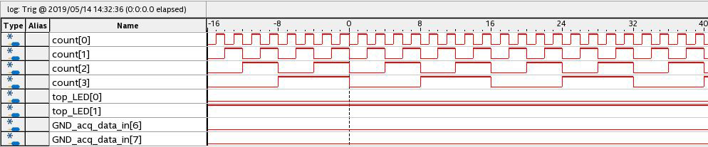
In this tutorial design, the count[3:0] signals represent the counter in the root partition, and the top_LED signals represent the green LEDs on the board, which also map to the top-level (root) design. After the trigger activates, only one of the top_LED bits is low, at any time.
If the root partition reuse succeeds, the Consumer project must present an identical behavior to the Developer project, since the Consumer imports the root partition .qdb file from this Developer project.
Related Information